

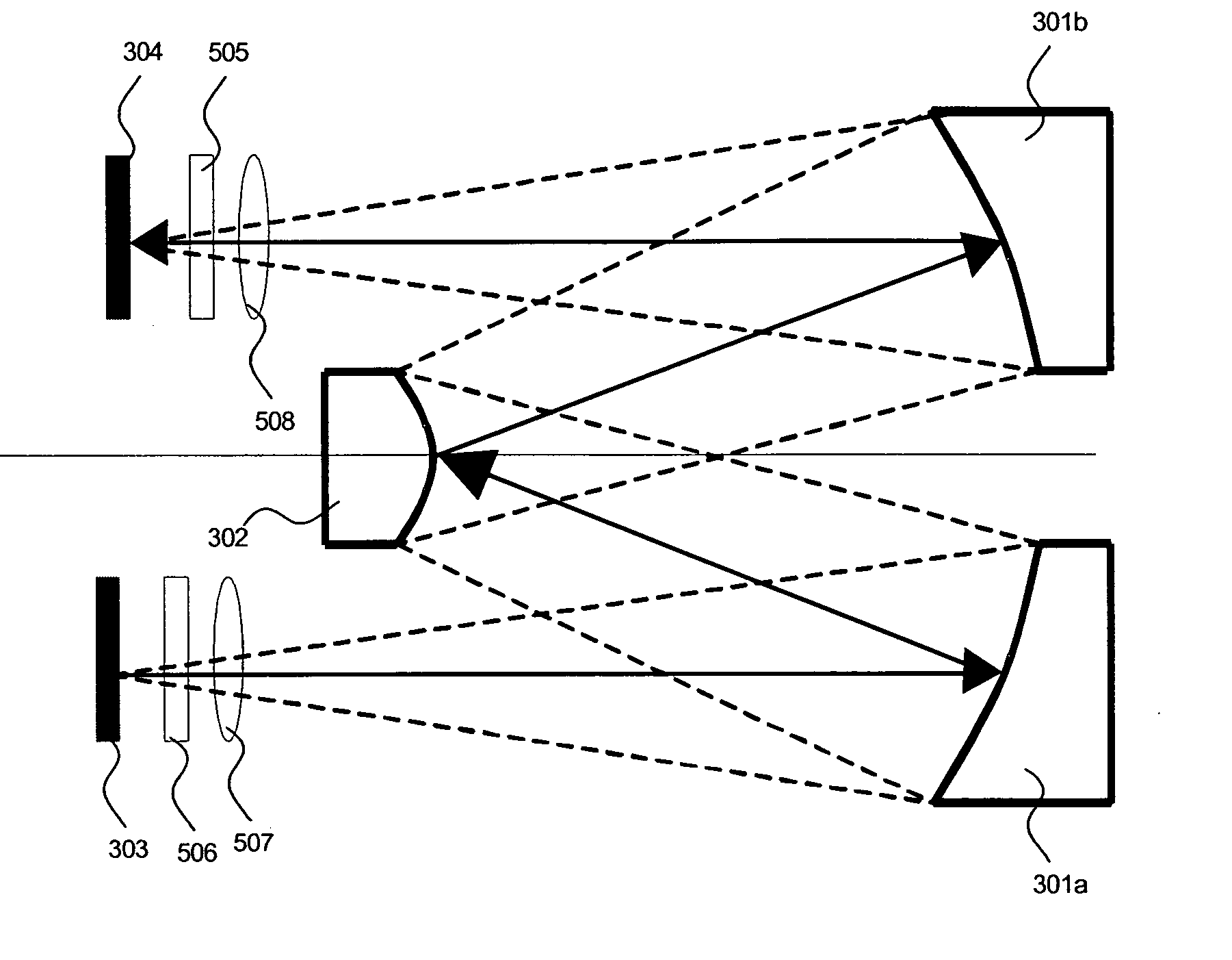
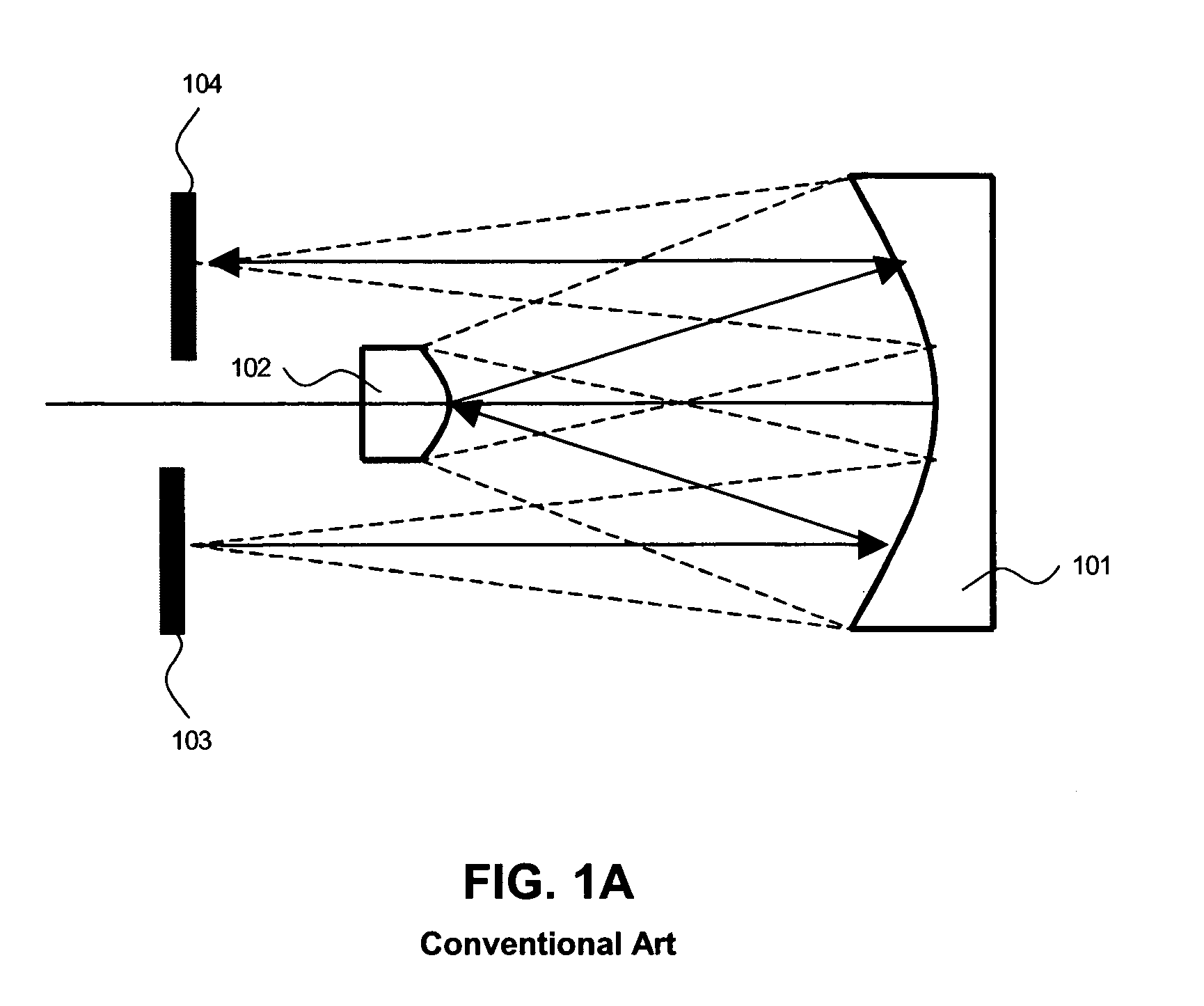
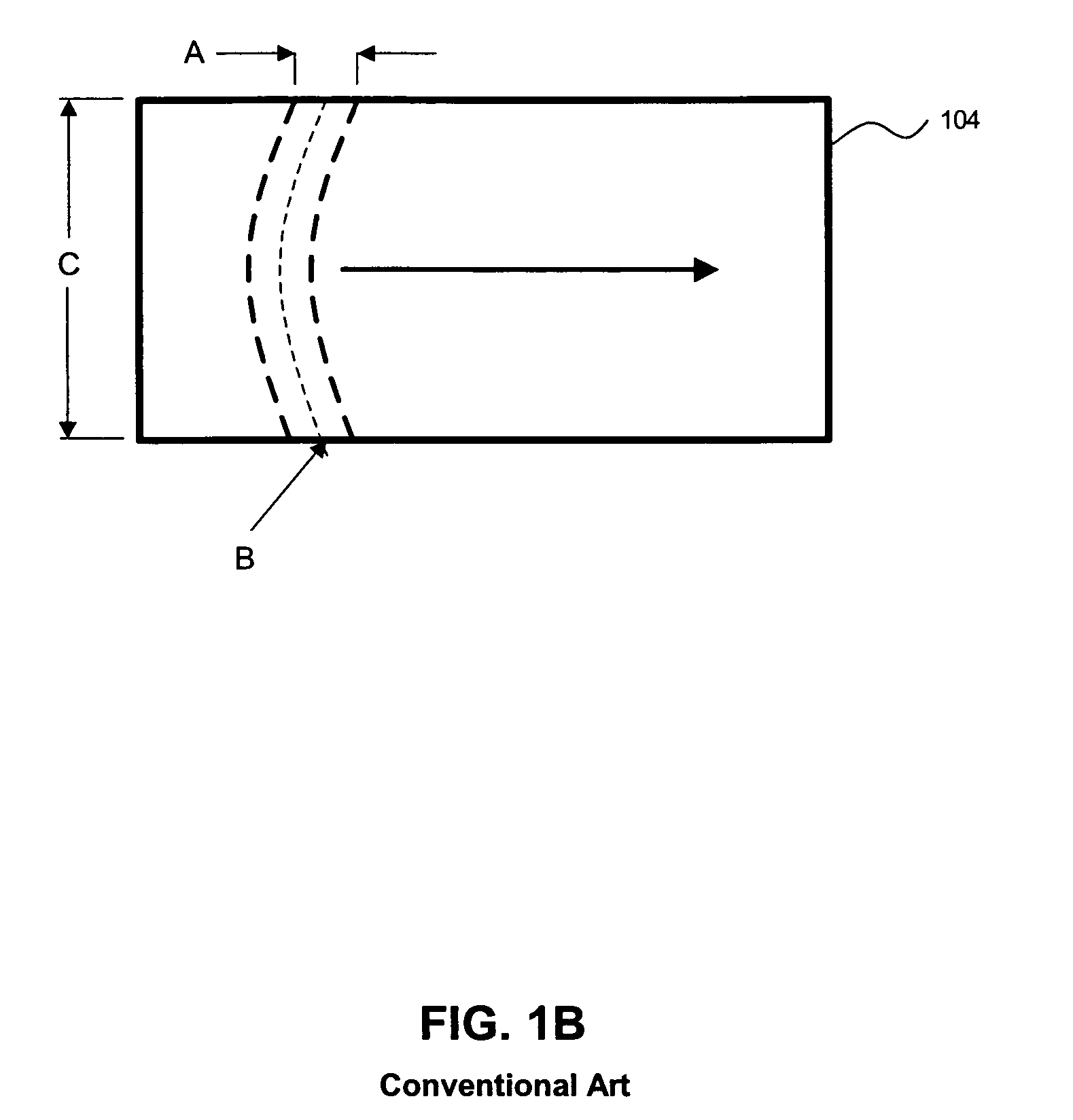
Large field of view protection optical system with aberration correctability for flat panel displays
a technology of optical system and aberration correctability, applied in the field of projection optical system, can solve problems such as unwanted aberrations, and achieve the effect of improving projection optics performan
- Summary
- Abstract
- Description
- Claims
- Application Information
AI Technical Summary
Benefits of technology
Problems solved by technology
Method used
Image

Examples
example 1
[0090]The table below gives exemplary optical prescription for Example 1:
[0091]
1X Optical Design Example #1 Optimized For Reduced VolumeRadiusDistanceConicAspheric CoefficientsSurface(mm)(mm)MaterialConstantY4Y6Y8Y10Object∞228.3Air0.00.00.00.00.0L1−460.730.0Fused0.0 2.1201 × 10⁻⁹ 3.8746 × 10⁻¹⁴−3.5049 × 10⁻¹⁹ 1.1333 × 10⁻²⁴SilicaL2−687.31583.3Air0.00.00.00.00.0M1−1186.8−721.8Reflection−0.9452−1.1717 × 10⁻¹¹−2.2769 × 10⁻¹⁹ 1.7648 × 10⁻²⁴−1.0603 × 10⁻³⁰M21065.0721.8Reflection−0.3065 6.6519 × 10⁻¹¹ 1.4057 × 10⁻²¹ 5.6254 × 10⁻²¹−1.3690 × 10⁻²⁵M3−1186.8−1583.3Reflection−0.9452−1.1717 × 10⁻¹¹−2.2769 × 10⁻¹⁹ 1.7648 × 10⁻²⁴−1.0603 × 10⁻³⁰L3−687.3−30.0Fused0.00.00.00.00.0SilicaLA−460.7−228.3Air0.0 2.1201 × 10⁻⁹ 3.8746 × 10⁻¹⁴−3.5049 × 10⁻¹⁹ 1.1333 × 10⁻²⁴Image
[0092]FIG. 7 shows a ray tracing diagram, and FIG. 8 shows the optical performance of the optical system of Example 1 in graphical form.
example 2
[0093]The table below gives exemplary optical prescription for Example 2 that uses refractive corrector elements:
[0094]
1X Optical Design Example #2 Optimized For Maximum Slit WidthRadiusDistanceConicAspheric CoefficientsSurface(mm)(mm)MaterialConstantY4Y6Y8Y10Object∞420.531Air0.00.00.00.00.0L1−207,468.930.0Fused Silica0.01.2258 × 10−9 −1.0071 × 10−155.7191 × 10⁻²² 2.3165 × 10⁻²⁸L2−161,733.82,049.470Air0.01.1629 × 10−9 −6.9811 × 10−151.2524 × 10−220.0M1−2,481.5−1,171.368Reflection0.08.4439 × 10−13−6.9104 × 10−213.5714 × 10−260.0M21065.01,171.368Reflection0.02.4939 × 10−12−3.0738 × 10−171.8895 × 10⁻²¹−3.2975 × 10⁻²⁶M3−2,481.5−2,049.470Reflection0.08.4439 × 10−13−6.9104 × 10−213.5714 × 10−260.0L3−161,733.8−30.0Fused Silica0.01.1629 × 10−9 −6.9811 × 10−151.2524 × 10−220.0L4−207,468.9−420.531Air0.01.2258 × 10−9 −1.0071 × 10−155.7191 × 10⁻²² 2.3165 × 10⁻²⁸Image
[0095]FIG. 9 shows a ray tracing diagram, and FIG. 10 shows the optical performance of the optical system of Example 2 in graphi...
PUM
| Property | Measurement | Unit |
|---|---|---|
| size | aaaaa | aaaaa |
| size | aaaaa | aaaaa |
| size | aaaaa | aaaaa |
Abstract
Description
Claims
Application Information