
Built-in self test system and method

a self-testing and built-in technology, applied in error detection/correction, digital storage, instruments, etc., can solve the problems of limited information from the bist test externally available to the chip, inability to distinguish between external testers, and high cost of silicon area

Active Publication Date: 2007-01-02
INFINEON TECH AG +1
View PDF9 Cites 20 Cited by
  • Summary
  • Abstract
  • Description
  • Claims
  • Application Information

AI Technical Summary

Benefits of technology

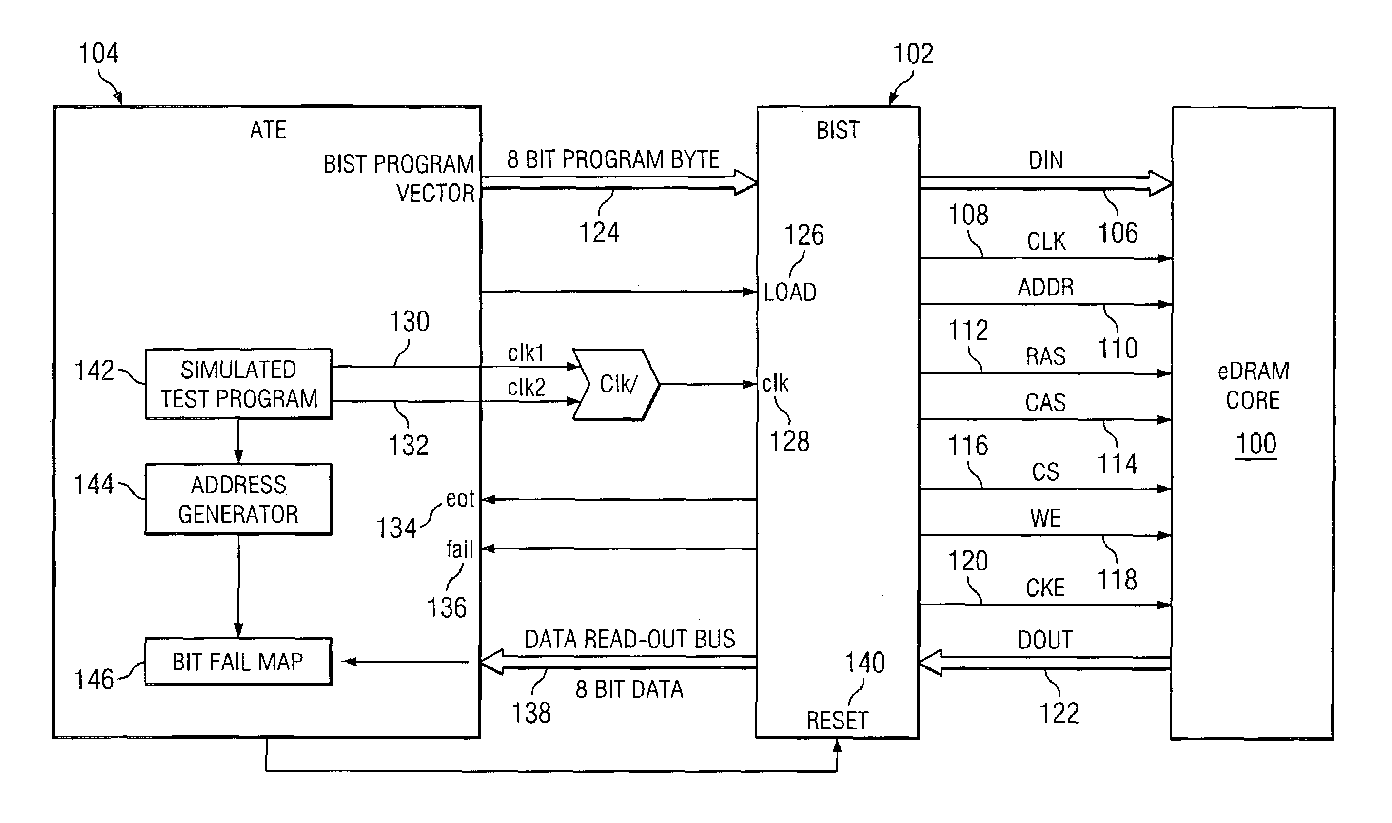
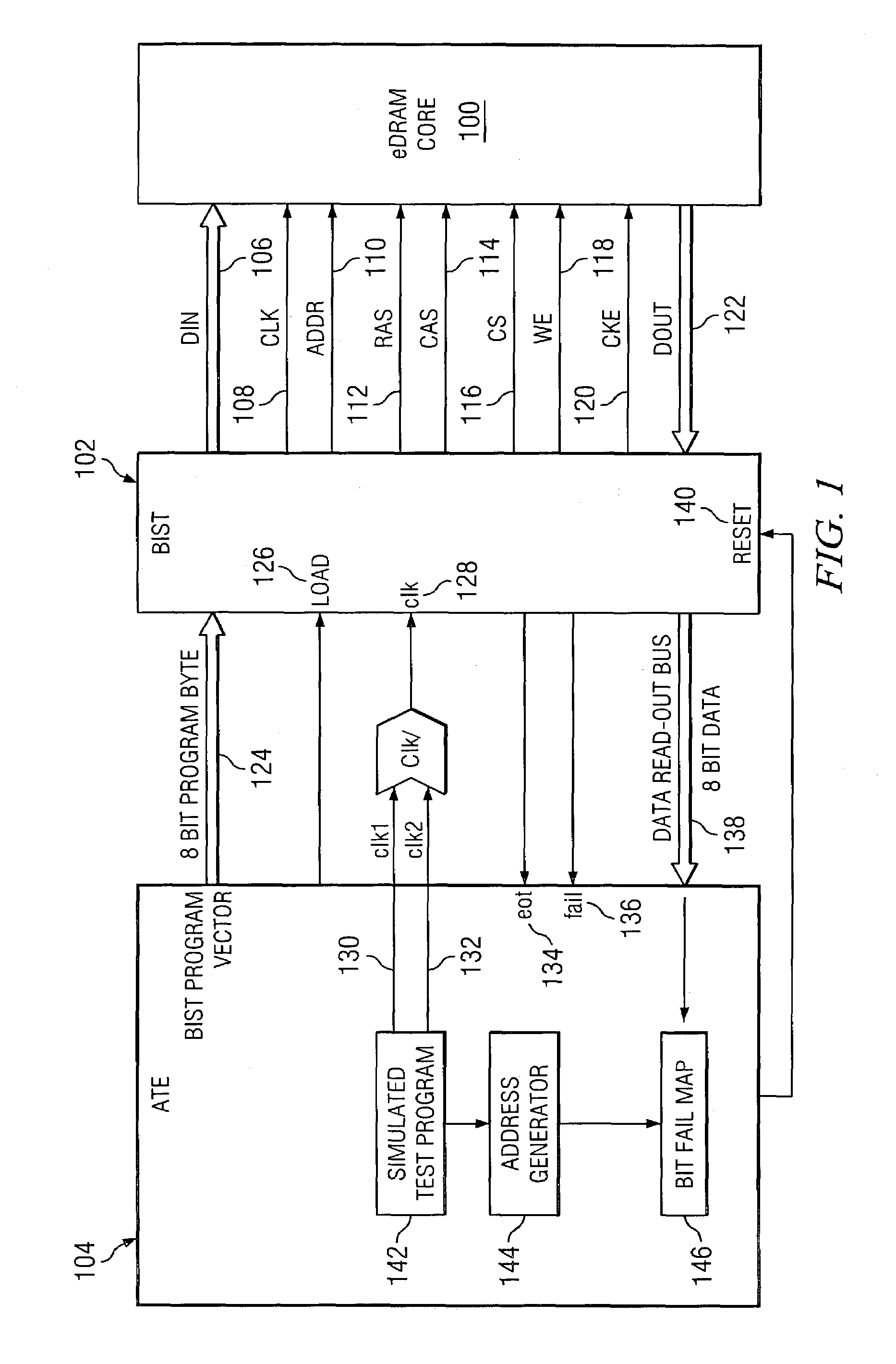
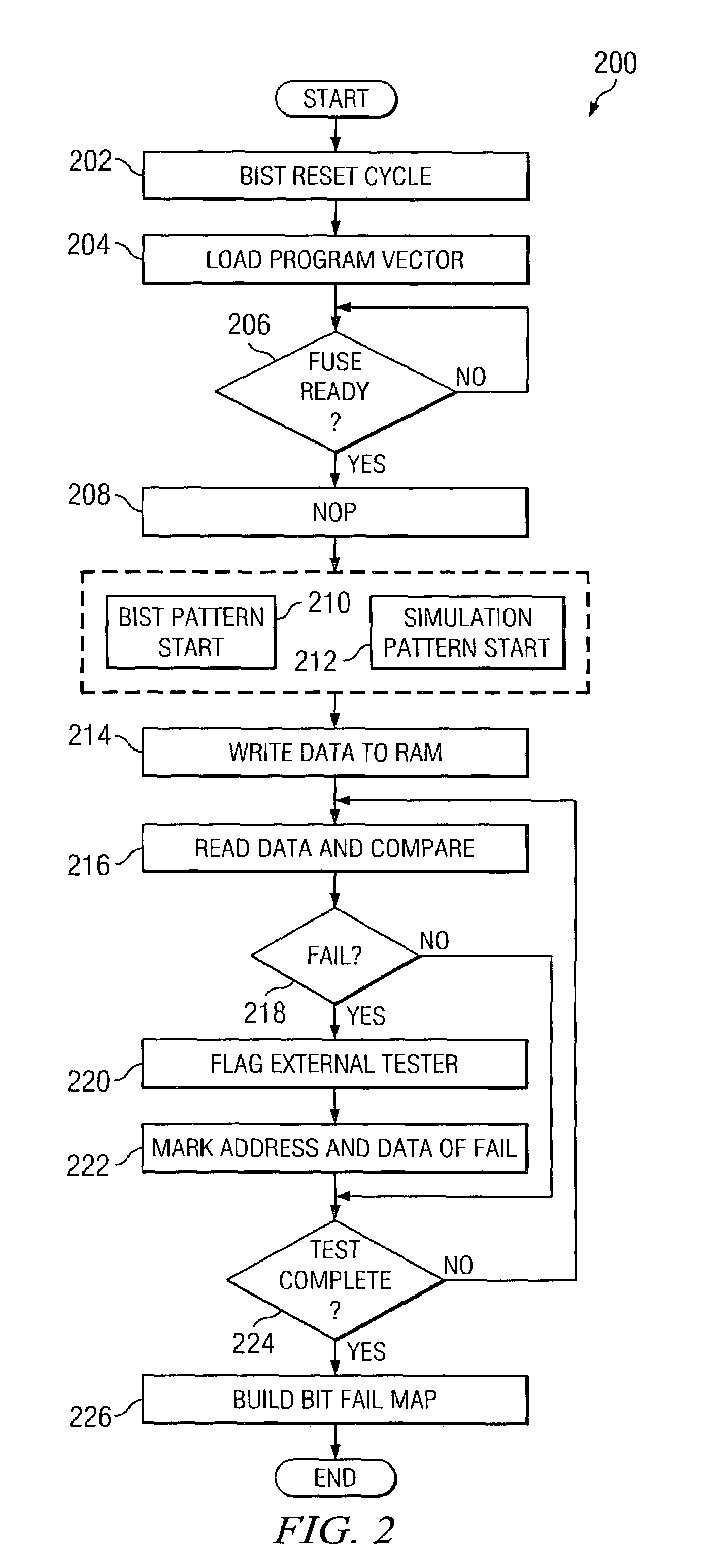
[0009]These and other problems are generally solved or circumvented, and technical advantages are generally achieved, by preferred embodiments of the present invention which utilize external test equipment to simulate the internal BIST test, thus enabling the capture or generation of detailed test results. By simulating the BIST test sequence in real time during the test, the external tester may monitor an output from the BIST and determine the exact location of failures when they occur. The external tester may generate a bit fail map to indicate whether each memory location passed or failed the BIST test.
[0013]An advantage of a preferred embodiment of the present invention is that it provides detailed information about the embedded memory core instead of just a single fail or pass. A bit fail map may be generated from a BIST test. The detailed information may indicate precisely where the fail or fails are occurring and just how much of the device is failing.
[0014]Another advantage of a preferred embodiment of the present invention is that it enables economical embedded memory testing because a manufacturer does not need to build a through pad memory test macro for line monitoring. The actual product with BIST may be used as the line monitor for detecting embedded memory defects.
[0015]Another advantage of a preferred embodiment of the present invention is that it allows at-speed testing of the embedded memory. The clock from the tester may be run at high speed to provide a realistic test of the device.

Problems solved by technology

Direct access testing for embedded eDRAM, or other types of embedded RAM such as embedded magnetic RAM (MRAM) and embedded flash RAM, however, generally is too costly in terms of silicon area, available input / output (I / O) pins, wiring complexity and test time.
One potential drawback associated with existing BIST implementations is that there is only limited information from the BIST test available externally to the chip.
In other words, the external tester receives the same result regardless of whether a single memory address on the chip fails, or the entire memory array fails, and the external tester cannot distinguish between the two, nor pinpoint the cause of the failure.

Method used


Image

  • Built-in self test system and method
  • Built-in self test system and method
  • Built-in self test system and method

Examples


Embodiment Construction

[0023]The making and using of the presently preferred embodiments are discussed in detail below. It should be appreciated, however, that the present invention provides many applicable inventive concepts that can be embodied in a wide variety of specific contexts. The specific embodiments discussed are merely illustrative of specific ways to make and use the invention, and do not limit the scope of the invention. For example, the embodiment described in detail below relates to BIST for an embedded DRAM core, but the invention may be utilized with other embedded circuits, such as other types of embedded memories, or other limited-access circuits on an ASIC.

[0024]FIG. 1 is a block diagram illustrating a test configuration in accordance with a preferred embodiment of the present invention. Embedded DRAM core 100 and BIST 102 are located on a semiconductor chip or die connected to automated test equipment (“ATE”) 104. Generally, full access to eDRAM core 100 is available on-chip, and onl...


PUM


Abstract

External test equipment is used to simulate an internal BIST test, thus enabling the capture or generation of detailed test results. By simulating the BIST test sequence in real time during the test, the external tester may monitor an output from the BIST and determine the exact location of failures when they occur. The external tester may generate a bit fail map indicating whether each memory location passed or failed the BIST test.

Description

TECHNICAL FIELD[0001]The present invention relates generally to a system and method for built-in self test (BIST), and more particularly to a system and method for real-time external simulation of BIST.BACKGROUND[0002]As Application Specific Integrated Circuit (ASIC) technologies expand into new markets, the need for denser embedded memory generally increases. For example, markets in portable and multimedia applications such as cellular phones and personal digital assistants generally demand increased density of embedded memory for higher function and lower power consumption. In order to accommodate this increased demand, embedded dynamic random access memory (eDRAM) macros have been offered in state-of-the-art ASIC portfolios. The integration of eDRAM into ASIC designs generally has intensified the focus on how best to test high-density macros, such as a complex DRAM macro, in a logic test environment.[0003]For example, direct memory access (DMA) testing generally may be used to te...

Claims


Application Information

Patent Timeline
Patent Type & Authority Patents(United States)
IPC IPC(8): G06F11/00G11C7/24G11C29/00G11C29/56H04B1/74
CPCG11C29/56G11C29/56004G11C2029/5606G11C2029/0401
Inventor WANG, LIDASAPPA, VASUDEVBOEHLER, THOMAS
Owner INFINEON TECH AG
Learn More