Display device and method for manufacturing the same

a technology for display devices and manufacturing methods, applied in static indicating devices, semiconductor/solid-state device details, instruments, etc., can solve the problems of high resistance of transparent conductive films, low power consumption of display devices disturbed, high resistance of electrodes, etc., to reduce the resistance of electrodes and wiring, reduce power consumption, and reduce the effect of wiring

Inactive Publication Date: 2007-01-09
SEMICON ENERGY LAB CO LTD
View PDF38 Cites 56 Cited by
  • Summary
  • Abstract
  • Description
  • Claims
  • Application Information

AI Technical Summary

Benefits of technology

[0010]Thus, an object of the present invention is to provide a display device which reduces substantial resistance of a second electrode, and which have a new configuration that can apply constant voltage to a light-emitting element.

Problems solved by technology

However, the resistance of the transparent conductive film is high.
As a result, it is concerned that low power consumption of the display device is disturbed.
However, as mentioned above, resistance of the second electrode is high, and consequently it is concerned that power consumption of a display device is increased.

Method used


Image

  • Display device and method for manufacturing the same
  • Display device and method for manufacturing the same
  • Display device and method for manufacturing the same

Examples


embodiment mode 1

(Embodiment Mode 1)

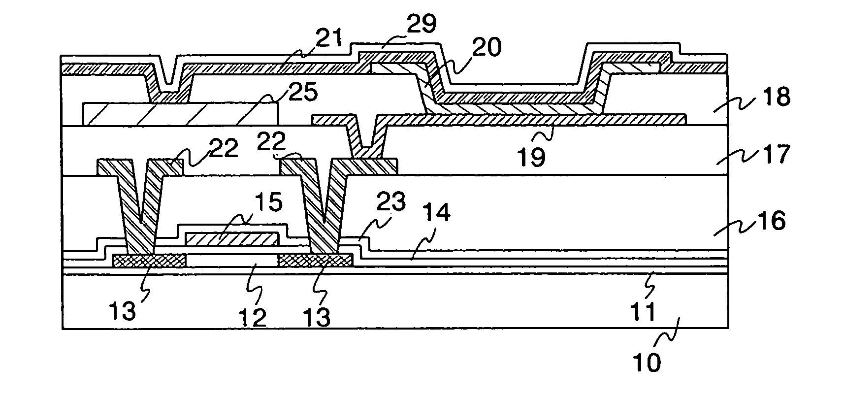
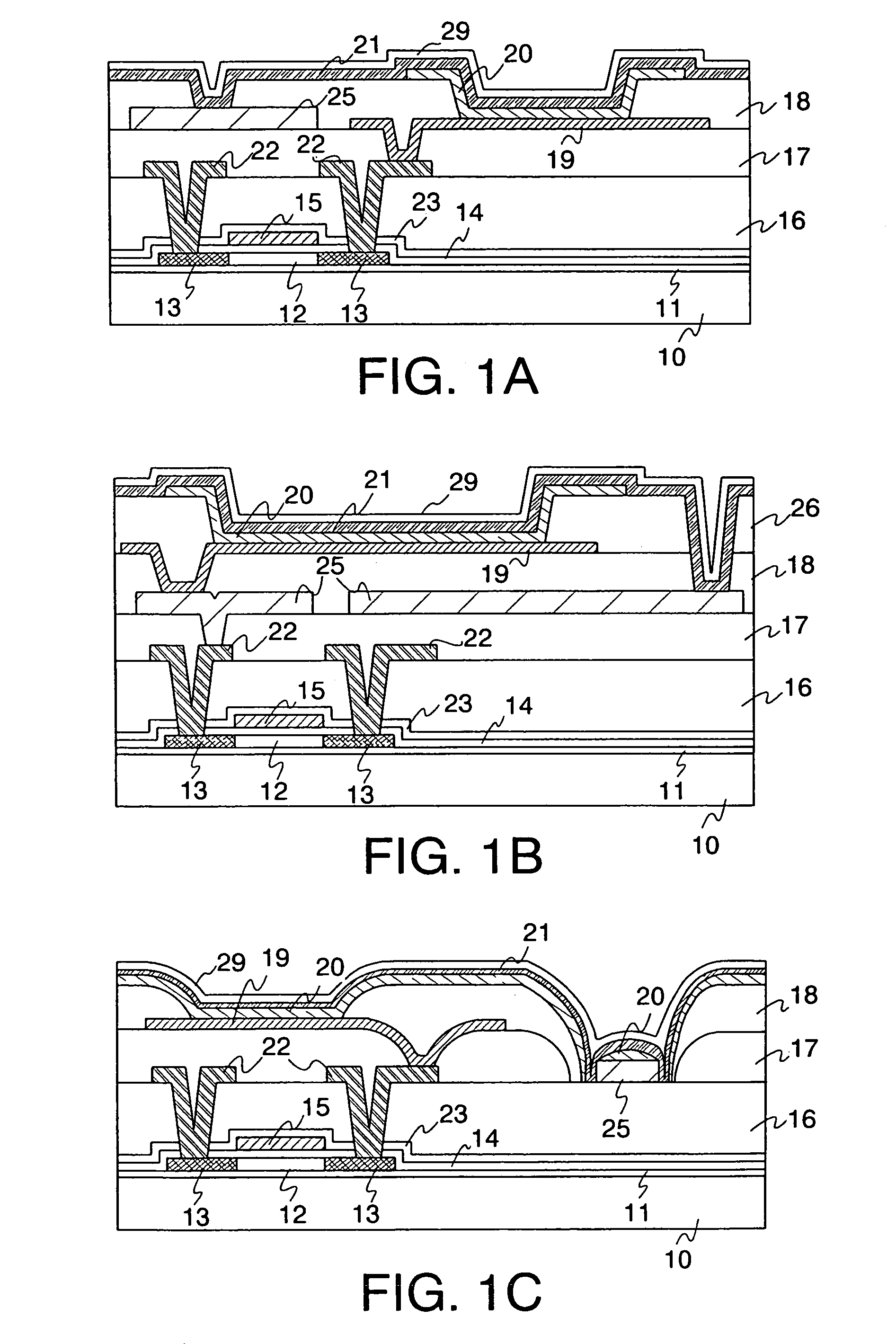
[0038]In this embodiment mode, a configuration of a pixel portion of a display device comprising an auxiliary wiring is described.

[0039]Configurations are shown in FIGS. 1A to 1C. That is, the configuration of a p-channel type TFT using polycrystalline silicon (polycrystalline TFT) as an example of a semiconductor element, and a pixel portion of the display device in which a transparent conductive film is employed as an example of the second electrode and in which the transparent conductive film that is a second electrode is connected to the auxiliary wiring.

[0040]In FIG. 1A, a configuration in which the second electrode is connected to the auxiliary wiring, and in which the auxiliary wiring is formed in one layer in which a first electrode is formed is shown. Note that the auxiliary wiring may be formed of either the same material as the first electrode or a different material.

[0041]The pixel portion of the display device comprises a base insulating film 11, a se...

embodiment mode 2

(Embodiment Mode 2)

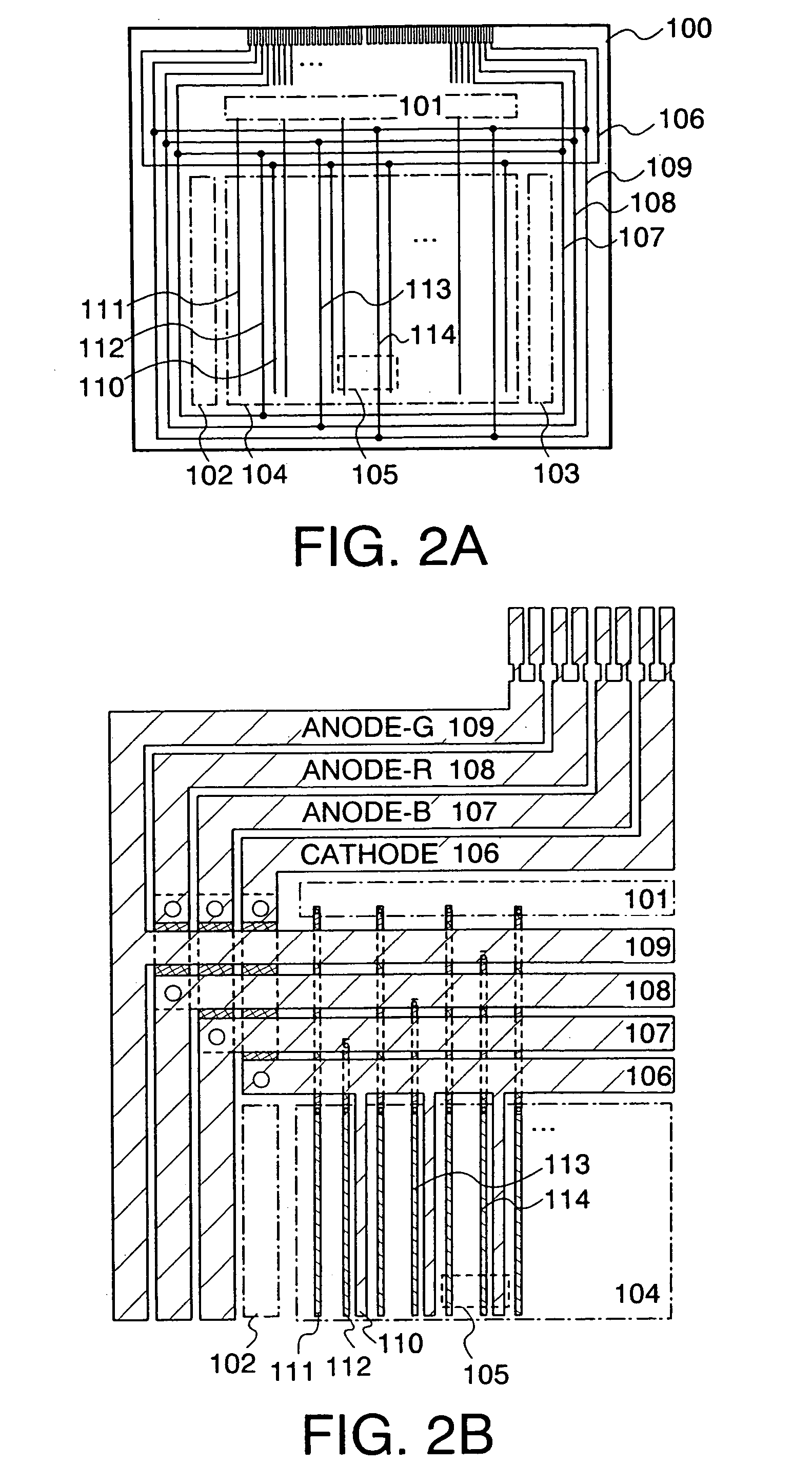
[0079]In this embodiment mode, an entire display device, especially, a lead wiring for connecting to an external circuit is described. Especially, a lead wiring with the same potential as high-potential voltage VDD (hereinafter, described as an anode line) and a lead wiring with the same potential as low-potential voltage VSS (hereinafter, described as a cathode line) are described with reference to FIGS. 2A and 2B. In FIGS. 2A and 2B, only a wiring disposed in a column direction in a pixel portion 104 is shown.

[0080]FIG. 2A is a top view of a panel, in which the pixel portion 104 where a plurality of pixels 105 are disposed in matrix a signal line driver circuit 101, and scanning line driver circuits 102 and 103 around the pixel portion 104 are disposed on a substrate. The number of these driver circuits is not limited to FIG. 2A, and a plurality of signal line driver circuits or a single scanning line driver circuit may be disposed according to a configuration o...

embodiment mode 3

(Embodiment Mode 3)

[0097]In this embodiment mode, an equivalent circuit of a pixel portion of a display device is described.

[0098]A pixel circuit shown in FIG. 7A comprises a light-emitting element 39, a signal line 30 in which a video signal is input, a transistor (switching transistor) 35 used for a switching element for controlling the input of the video signal into a pixel, a transistor (drive transistor) 36 for controlling current value flown into the light-emitting element 39, a transistor (current control transistor) 37 for controlling the supply of current to the light-emitting element 39, and an auxiliary wiring 34 connected with a second electrode of the light-emitting element 39. Furthermore, a capacitor element 38 for holding the potential of the video signal may be provided.

[0099]The drive transistor 36 and the current control transistor 37 are formed so as to have a same conductivity type. This embodiment mode describes the case of a p-channel type.

[0100]In this embodi...


PUM


Abstract

An object of the present invention is to decrease substantial resistance of an electrode such as a transparent electrode or a wiring, and furthermore, to provide a display device for which is possible to apply same voltage to light-emitting elements. In the invention, a auxiliary wiring that is formed in one layer in which a conductive film of a semiconductor element such as an electrode, wiring, a signal line, a scanning line, or a power supply line is connected to an electrode typified by a second electrode, and a wiring. It is preferable that the auxiliary wiring is formed into a conductive film to include low resistive material, especially, formed to include lower resistive material than the resistance of an electrode and a wiring that is required to reduce the resistance.

Description

BACKGROUND OF THE INVENTION[0001]1. Field of the Invention[0002]The present invention relates to a display device equipped with a light-emitting element and a method for manufacturing the same.[0003]2. Description of the Related Art[0004]In recent years, a large-sized screen and high-definition are promoted in a display device having a light-emitting element and a liquid crystal element, which the number of wirings such as a signal line and a scanning line, and the length of a wiring tend to increase. Therefore, it is necessary to prevent voltage drop due to wiring resistance, a signal writing defect, a gradation defect, and the like.[0005]Thus, there is a configuration in which an auxiliary wiring made of a transparent conductive film is connected to the transparent electrode that the light-emitting element has, interposing an anisotropical conductor (refer to Patent Document 1). According to Patent Document 1, effective resistance of the transparent electrode can be lowered. Furth...

Claims


Application Information

Patent Timeline
Patent Type & Authority Patents(United States)
IPC IPC(8): H01L29/04H01L31/036H01L31/0376H01L31/20H01L33/00G09G3/32H01L27/32H01L51/52
CPCG09G3/3233G02F1/133345H01L51/5206H01L51/5221H01L27/3276G09G2300/0842G09G2300/0861H01L2251/5315H10K59/131H10K50/81H10K50/824H10K50/828H10K2102/3026H10K50/82H10K50/814H10K59/1315H01L23/5228H01L27/1222H01L27/124H01L27/1248H01L33/40
Inventor MIYAGI, NORIKOSAKAKURA, MASAYUKIARAO, TATSUYANAGAO, RITSUKOTANADA, YOSHIFUMI
Owner SEMICON ENERGY LAB CO LTD
Why Eureka
Try Eureka