

Semiconductor device
a technology of semiconductor chips and semiconductor chips, applied in the field of semiconductor devices, can solve the problems of increasing the output circuit size, and the inability to manufacture high-density semiconductor chips with a reduced output circuit size by combining conventional technologies, and achieve the effect of reducing the area of the output circui
- Summary
- Abstract
- Description
- Claims
- Application Information
AI Technical Summary
Benefits of technology
Problems solved by technology
Method used
Image

Examples
first embodiment
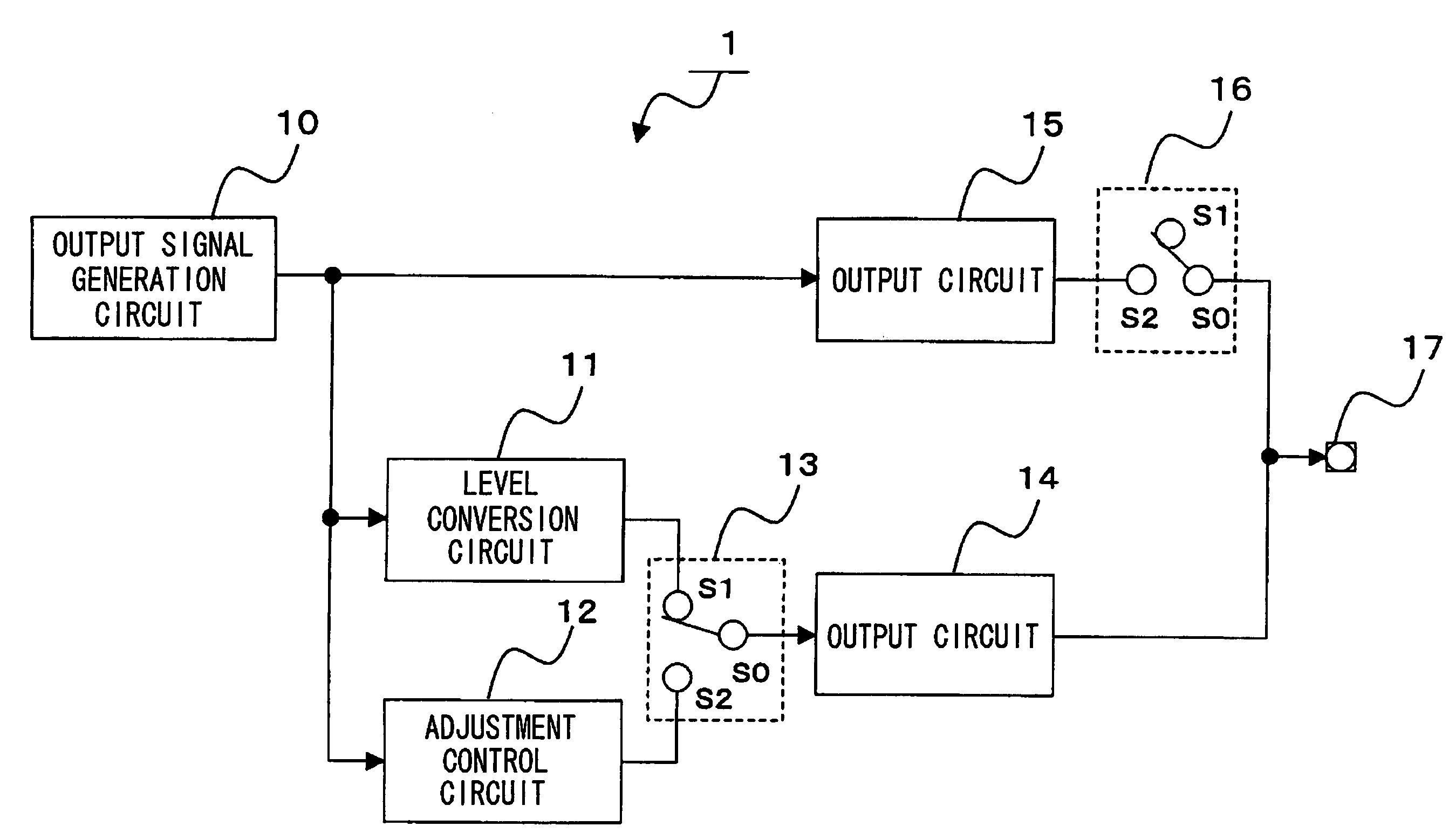
[First Embodiment]
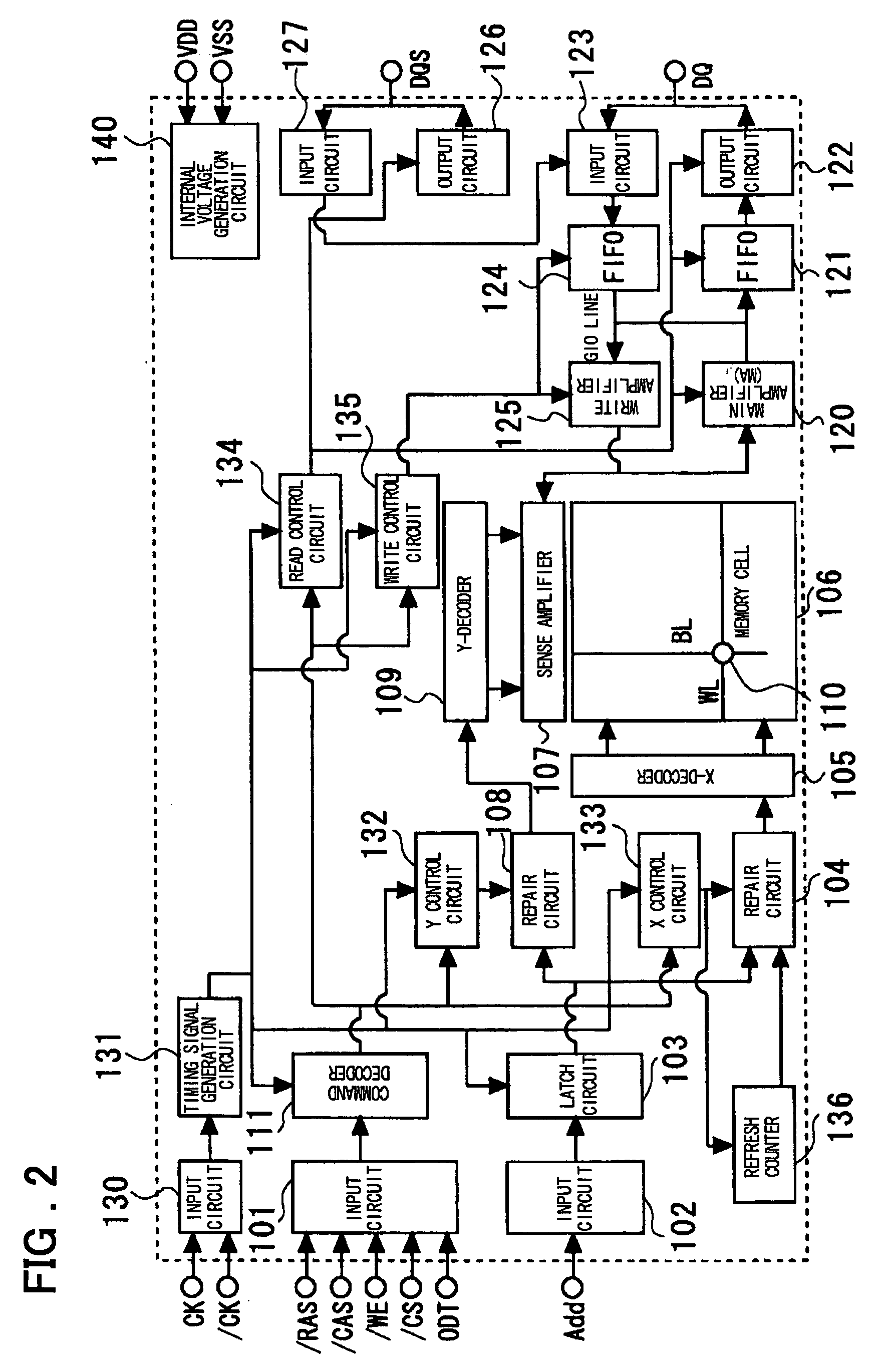
[0032]A DDR SDRAM will be described as an example in which the present invention is applied. FIG. 2 is a diagram showing an example of the whole block configuration of a DDR SDRAM. In the description below, the symbol “ / ” indicates an inversion bar (over-bar) to show that the low level is an active level.
[0033]The control input signals are a row address strobe signal / RAS, a column address strobe signal / CAS, a write enable signal / WE, a chip select signal / CS, and an on-die termination adjustment signal ODT. Those signals are input to an input circuit 101. The signals output from the input circuit 101 are sent to a command decoder 111 in synchronization with a timing signal generated by a timing signal generation circuit 131 and, based on the decoding result, distributed to an X control circuit 133, a Y control circuit 132, a read control circuit 134, and a write control circuit 135.
[0034]Clock signals CK and / CK are input to an input circuit 130. A timing signal ...
second embodiment
[Second Embodiment]
[0079]Next, the following describes an example in which a special output circuit is provided and a part of the adjustment circuit for DDR2 is combined with the output circuit when the SDRAM is a DDR1 SDRAM. FIG. 5 is a block diagram showing a semiconductor device in a second embodiment of the present invention. In FIG. 5, the same reference numerals as those in FIG. 1 denote the same structural elements. The following primarily describes the new elements, but obviating the explanation of the elements with the same reference numerals. A semiconductor device 1 comprises a third output circuit 19 and a switch 18. The output of a level conversion circuit 11 is connected to a third output circuit 19, and the output of the third output circuit 19 is connected to contact S1 of the switch 18. The switch 18 is the same as the switch 16 in FIG. 1 except the connection of contact S1. A first output circuit 14a has a function similar to that of the first output circuit 14 in ...
third embodiment
[Third Embodiment]
[0093]Next, the following describes another example of a detailed circuit that implements the function of the block diagram shown in FIG. 5. FIG. 7 is a circuit diagram showing the output circuit of a DDR-1 / DDR-2 compatible SDRAM chip in a third embodiment of the present invention. In the circuit shown in FIG. 7, the same reference numerals as those in FIG. 6 denote the same or equivalent structural elements. The following primarily describes the new elements, but not the elements with the same reference numerals.
[0094]In an OCD adjustment circuit 42b, the transistors Q17 and Q18 of the OCD adjustment circuit 42 in the first embodiment are replaced, respectively, by low-breakdown voltage transistor Q29 and Q30 and switches SW27 and SW28 are provided. When the SDRAM is a DDR1 SDRAM, the drains of the transistors Q29 and Q30 are connected to the power supply VDDQ and the ground VSSQ, respectively; when the SDRAM is a DDR2 SDRAM, the drains of the transistors Q29 and ...
PUM
 Abstract
Description
Claims
Application Information