Laser-irradiated thin films having variable thickness

a technology of variable thickness and laser irradiation, which is applied in the direction of crystal growth process, chemistry apparatus and processes, manufacturing tools, etc., can solve the problems of inefficiency and uneconomical processing of the entire film surface, and the inability to meet the high mobility requirements of the integration region,

Inactive Publication Date: 2007-01-16
THE TRUSTEES OF COLUMBIA UNIV IN THE CITY OF NEW YORK
View PDF184 Cites 89 Cited by
  • Summary
  • Abstract
  • Description
  • Claims
  • Application Information

AI Technical Summary

Problems solved by technology

The process typically uses a long, narrow beam shape that is continuously advanced over the substrate surface, so that the beam can potentially irradiate the entire semiconductor thin film in a single scan across the surface ELA produces homogeneous small grained polycrystalline films; however, the method often suffers from microstructural non-uniformities which can be caused by pulse to pulse energy density fluctuations and / or non-uniform beam intensity profiles.
Processing the entire film surface, e.g., the integration regions and the pixel regions, under the conditions necessary to meet the high mobility requirements of the integration regions can be inefficient and uneconomical since excess irradiation and processing time of the lower performance regions of the thin film may have been expended with no gain in system performance.

Method used


Image

  • Laser-irradiated thin films having variable thickness
  • Laser-irradiated thin films having variable thickness
  • Laser-irradiated thin films having variable thickness

Examples


Embodiment Construction

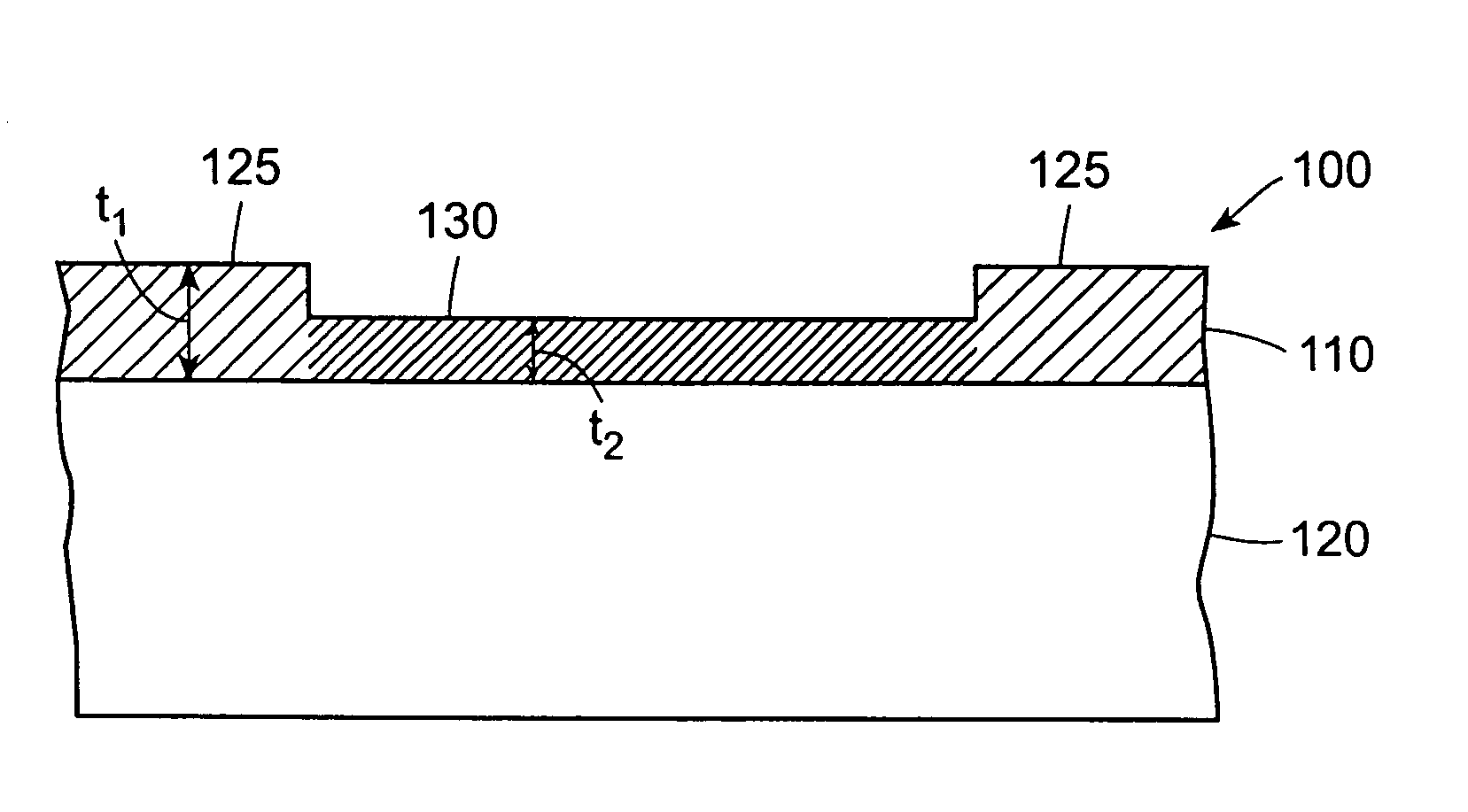
[0027]The quality of a film that has been crystallized using a laser-induced crystallization growth technique depends, in part, on the thickness of the processed film. This observation is used to crystallize different regions of the film in an energy- and time-efficient manner and to provide a desired film characteristic. Laser-induced crystallization is typically accomplished by laser irradiation using a wavelength of energy that can be absorbed by the film. The laser source may be any conventional laser source, including but not limited to, excimer laser, continuous wave laser and solid-state laser. The irradiation beam pulse can be generated by other known sources for short energy pulses suitable for melting a semiconductor or metallic material. Such known sources can be a pulsed solid state laser, a chopped continuous wave laser, a pulsed electron beam and a pulsed ion beam, and the like.

[0028]Films of different thicknesses, although similarly processed, have different film prop...


PUM

PropertyMeasurementUnit
thicknessaaaaaaaaaa
thicknessaaaaaaaaaa
lengthaaaaaaaaaa

Abstract

A crystalline film includes a first crystalline region having a first film thickness and a first crystalline grain structure; and a second crystalline region having a second film thickness and a second crystalline grain structure. The first film thickness is greater than the second film thickness and the first and second film thicknesses are selected to provide a crystalline region having the degree and orientation of crystallization that is desired for a device component.

Description

CROSS-REFERENCE TO RELATED APPLICATIONS[0001]This patent application claims priority under 35 U.S.C. § 119(e) to U.S. Provisional Patent Application Ser. No. 60 / 503,424 filed Sep. 16, 2003, which is hereby incorporated by reference.FIELD OF THE INVENTION[0002]This invention relates to methods and systems for processing thin films, and more particularly to forming crystalline semiconductor thin films from amorphous or polycrystalline thin films using laser irradiation. In particular the present invention relates to a method and system for the production of integrated thin film transistors.BACKGROUND OF THE INVENTION[0003]In recent years, various techniques for crystallizing or improving the crystallinity of an amorphous or polycrystalline semiconductor film have been investigated. This technology is used in the manufacture of a variety of devices, such as image sensors and active-matrix liquid-crystal display (AMLCD) devices. In the latter, a regular array of thin-film transistors (T...

Claims


Application Information

Patent Timeline
Patent Type & Authority Patents(United States)
IPC IPC(8): H01L29/04H01L31/036H01L21/20H01L21/268
CPCH01L21/2026B23K26/08B23K26/0042H01L21/268H01L21/02532H01L21/02678H01L21/02683H01L21/02686C30B1/00H01L21/84H01L29/04
Inventor IM, JAMES
Owner THE TRUSTEES OF COLUMBIA UNIV IN THE CITY OF NEW YORK
Why Eureka
Try Eureka