Self-scrub buckling beam probe

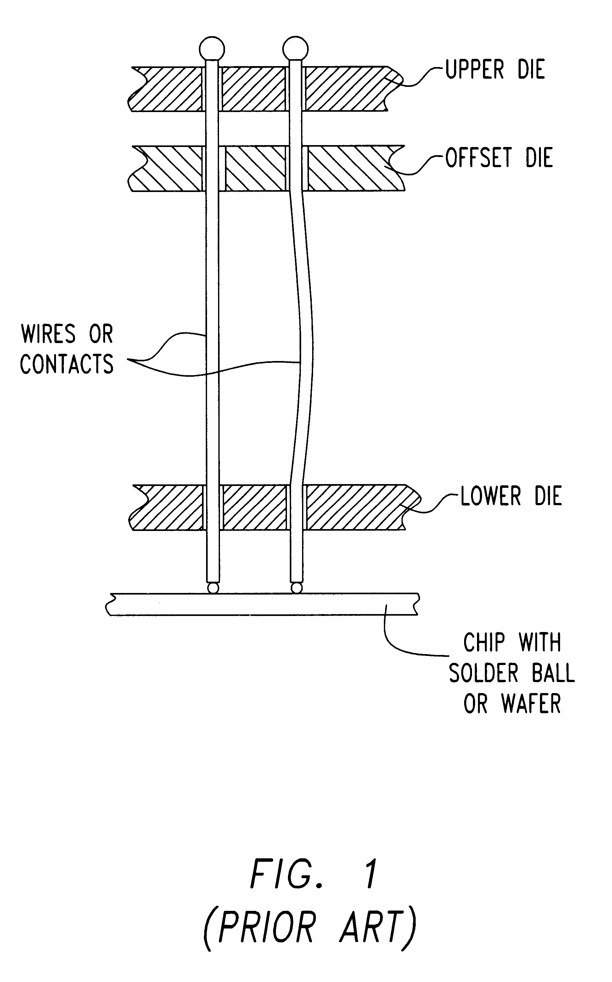
a beam probe and self-scrubbing technology, applied in the direction of coupling device details, coupling device connection, instruments, etc., can solve the problems of destroying the pad altogether, difficult to design probes with more than one layer, and difficult to physically position them without, so as to reduce the resistance and prevent contaminants

Inactive Publication Date: 2003-03-04
IBM CORP
View PDF4 Cites 54 Cited by
  • Summary
  • Abstract
  • Description
  • Claims
  • Application Information

AI Technical Summary

Benefits of technology

When a reciprocating motion to the tip of the wire is applied when the wires contact the surface of the device under test, a scrubbing motion is achieved that lowers the resistance between the pad of the device under test. In this manner, the tip of the wire cleans the surface of the pads and prevents contaminants from adhering to the tip of the wire.

Problems solved by technology

Oftentimes, excessive force exerted by the probe on the pad, particularly when dealing with a chip, can destroy the pad altogether, requiring the additional step of having to reconstruct the pad in question by way of techniques known as solder reflow.
Such probes with more than one layer are difficult to design, specifically having a plurality of probe tips to be coplanar for allowing contact to all the pads of an array with equal force.
Even when multiple layers of probes are used, it is still difficult to physically position them without they interfering with each other.
A limited amount of wiping (scrubbing) of the pads of the device under test is achievable, although the construction of the Cobra probe precludes an effective wiping action which is essential to establish good contact with the pads because of its characteristic low inertia and vertical retention.
The problem associated with vertical only movement probe is that when probing is performed on Al pads, as typically found in semiconductor wafers, the probe does not easily penetrate and push off the oxide layer on the pad, resulting in a high and unstable contact resistance.

Method used


Image

  • Self-scrub buckling beam probe
  • Self-scrub buckling beam probe
  • Self-scrub buckling beam probe

Examples


Embodiment Construction

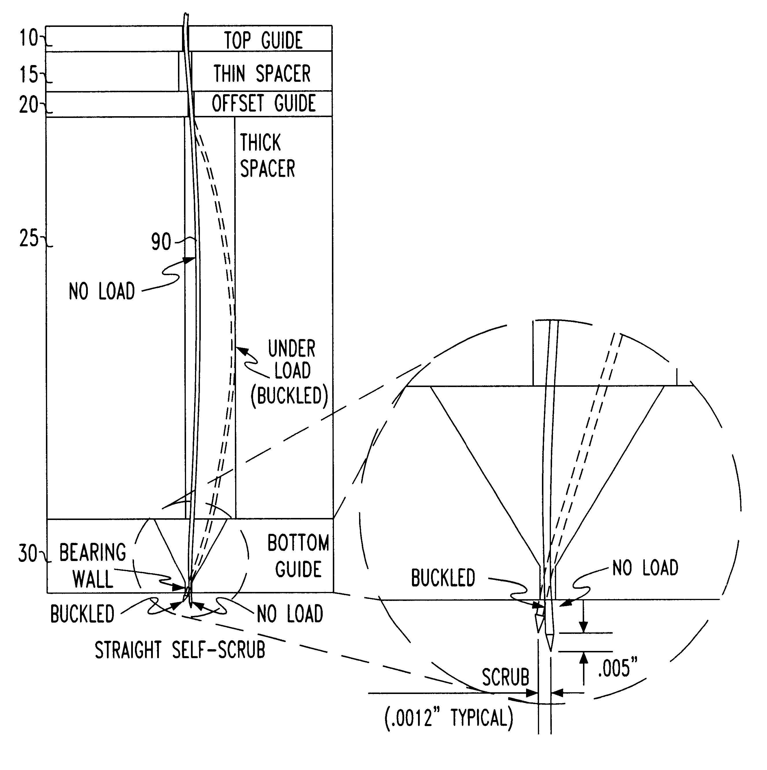
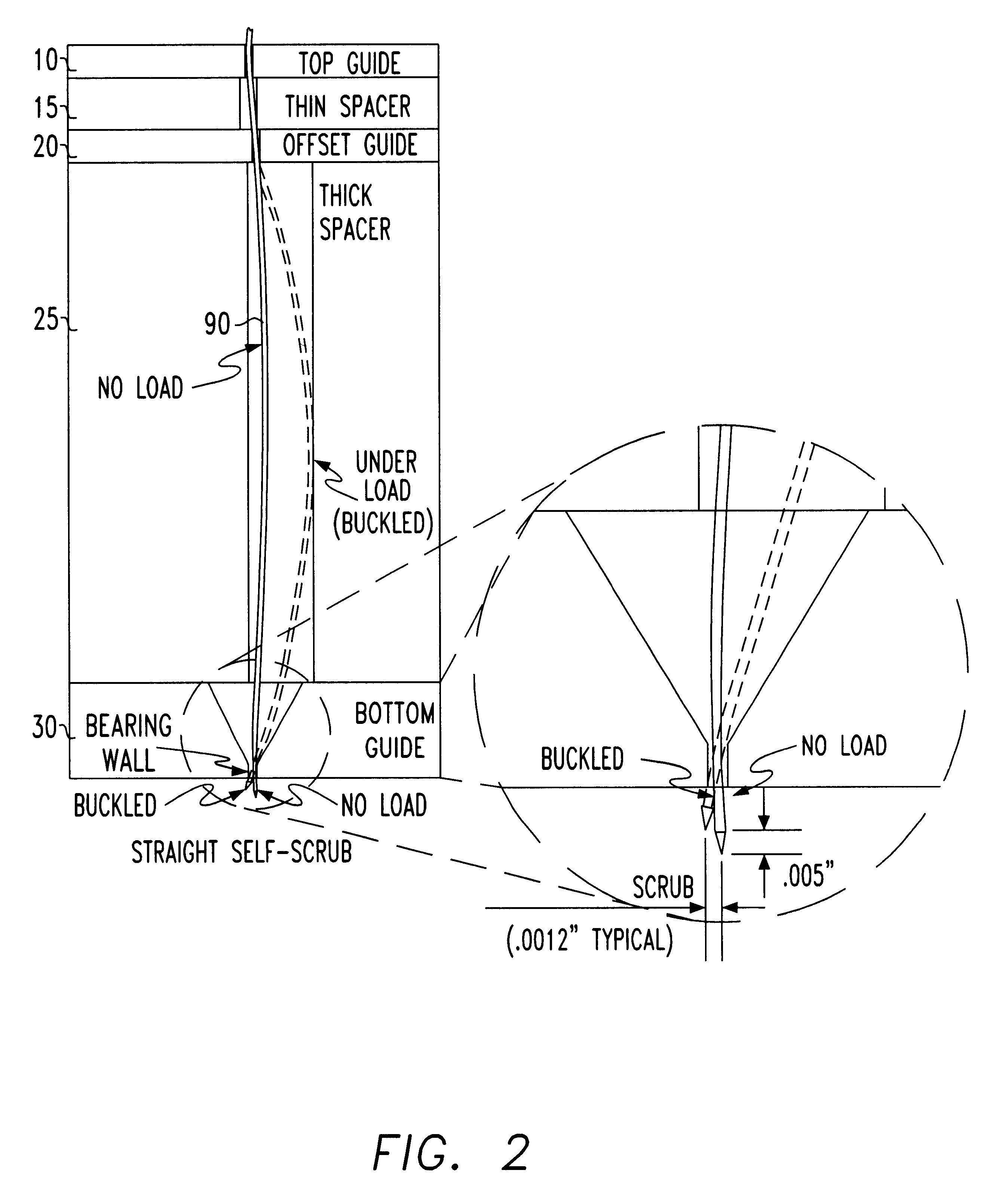
Referring now to the drawings, and more particularly to FIG. 2, there is shown a side view of a straight self-scrub buckling beam and an exploded view of its tip, in accordance with the invention. The beam is shown both, in a no load state as well as under compressive stress, to be referred hereinafter as a buckled beam.

An array of electrically conductive contacts made of thin straight wires 90 are held by three insulated guide plates. These are: a top guide plate (or die) 10, an offset guide plate 20 and a bottom guide plate 30. The guide plates are typically provided with an array of round holes having the same pitch as the footprint of the Device under Test (DUT). The diameter of the holes is slightly larger than those of the probe to allow a vertical displacement under load. The offset guide 20 hole pattern is offset by dowel pins in a predetermined direction, normally a few thousandths of an inch, in order to force the beam to buckle in a set direction. The guide plates are sep...


PUM


Abstract

A self scrubbing buckling beam contactor for contacting an array of pads positioned on a device under test is described. The contactor consists of three insulating dies: a top, an offset and a lower die separated from each other by an insulated spacer of variable thickness. Each die is provided with holes. The buckling beam has an array of flexible wires positioned substantially perpendicular to the dies, each of the flexible wires crossing a corresponding hole in each of the top, offset and lower dies to allow each wire respectively contact a pad of the device under test. By shifting the center of the hole of the lower die relative to the center of the offset die, the tip of the wire exits from the lower die at an angle with respect to the plane formed by the pads of the device under test. The exit angle of the wire tip is controlled by the relative displacement of the offset die relative to the bottom die, such that the exit angle of the tip of the wire at the bottom die changes when the probe wire is under compression. By applying a reciprocating motion to the tip of the wire contacting the surface of the device under test, a scrubbing motion is achieved that lowers the resistance between the pad of the device under test. In this manner, the tip of the wire cleans the surface of the pads and prevents contaminants from adhering to the tip of the wire.

Description

This invention is related to a probe contactor having a plurality of buckling beams, and more particularly to a probe provided with self-scrubbing features such that when a force is applied to the probe, the tip of the probe changes its landing angle, providing a controlled scrub by wiping action.Present trends in the microelectronic industry portend ever increasing chip densities, which translate in the need for new probing devices to accommodate the increase in the number of I / O pads.When testing the electrical characteristics of an integrated circuit, whether a chip, module, and the like, the probes of a contactor engage the pads of the package under test to provide an electric path from the device under test to the tester. Accordingly, it is imperative to ensure that the probes contacting the pads be endowed with a controlled force to prevent or at the least, reduce, any damage to the pads. Oftentimes, excessive force exerted by the probe on the pad, particularly when dealing wi...

Claims


Application Information

Patent Timeline
Patent Type & Authority Patents(United States)
IPC IPC(8): G01R1/073
CPCG01R1/07357G01R1/07314
Inventor YU, YUET-YINGBERGER, DANIEL GBOWNE, CAMILLE PROIETTILANGENTHAL, SCOTTPERRY, CHARLES HSPOOR, TERENCEWEISS, THOMAS
Owner IBM CORP
Why Eureka
Try Eureka