Light emitting display, display panel, and driving method thereof

a technology of light-emitting display and display panel, which is applied in the direction of static indicating devices, instruments, solid-state devices, etc., can solve the problems of difficult to obtain high gray, difficult to represent high gray, and the control of the pixel circuit by fine current i/sub>data problem requires a lot of time to charge the data line, so as to achieve fast timing and high uniformity between the threshold voltages of the first and second transistors

Active Publication Date: 2007-01-16
SAMSUNG DISPLAY CO LTD
View PDF13 Cites 25 Cited by
  • Summary
  • Abstract
  • Description
  • Claims
  • Application Information

AI Technical Summary

Benefits of technology

[0022]In one aspect of the present invention, a light emitting display is provided on which a plurality of data lines for transmitting data current that displays video signals, a plurality of scan lines for transmitting a select signal, and a plurality of pixel circuits formed at a plurality of pixels defined by the data lines and the scan lines are formed. The pixel circuit includes: a light emitting element for emitting light corresponding to the applied current; a first transistor, having first and second main electrodes and a control electrode, for supplying a driving current for the light emitting element a second transistor being diode-connected; a first switch for transmitting a data current from the data line to the second transistor in response to a select signal from the scan line; a first storage element having a first end coupled to the first main electrode of the first transistor and a first main electrode of the second transistor, and a second end thereof coupled to the control electrode of the first transistor, the second end being coupled to a gate of the second transistor in response to a first level of a first control signal; a second storage element coupled between the second end of the first storage element and a control electrode of the second transistor in response to a second level of the first control signal; and a second switch for coupling the first transistor and the light emitting element in response to a second control signal. The light emitting display operates in the order of a first interval for selecting the first level of the first control signal and the select signal, a second interval for selecting the second level of the first control signal, and a third interval for selecting the second control signal. The voltage of the control electrode of the second transistor is determined as a first voltage in correspondence with the data current in the first interval. A control electrode voltage of the second transistor is changed to a second voltage from the first voltage by the interception of the data current. A control electrode voltage of the first transistor is determined as a third voltage by coupling of the first and second storage elements to store a fourth voltage in the first storage element in the second interval. A driving current corresponding to the fourth voltage is transmitted to the light emitting element from the first transistor in the third interval. The pixel circuit further includes a third switch coupled between the control electrodes of the first and second transistors. The third switch is turned on by the first level of the first control signal. The first control signal is the select signal. The first control signal is supplied from an additional signal line other than the scan line, and the first control signal has faster timing than the select signal. A channel width of the first transistor is equal to or shorter than the channel width of the second transistor. A channel length of the first transistor is equal to or longer than the channel width of the second transistor. The first storage element is a first capacitor formed between the first main electrode and the control electrode of the first transistor. The second storage element is a second capacitor formed between the control electrodes of the first and second transistors. Capacitance of the first capacitor and capacitance of the second capacitor is determined by one of a screen size and resolution. Uniformity between the threshold voltages of the first and second transistors is high.
[0023]In another aspect of the present invention, a method is provided for driving a light emitting display having a pixel circuit including a first switch for transmitting a data current from a data line in response to a select signal from a scan line, a first transistor including first and second main electrodes and a control electrode for outputting a driving current corresponding to the data current, a first storage element formed between the first main electrode and the control electrode of the first transistor, and a light emitting element for emitting light corresponding to the driving current from the first transistor. The control electrode of the diode-connected second transistor is coupled to the control electrode of the first transistor. The data current is transmitted from the first switch to the second transistor to establish the control electrode voltage of the second transistor as a first voltage. A second storage element is formed between the control electrodes of the first and second transistors. Data current is intercepted to modify the first voltage into a second voltage to which a threshold voltage of the second transistor is reflected. Coupling of the second voltage and the first and second storage elements is used to modify the control electrode voltage of the first transistor into a third voltage from the first voltage. A driving current output is transmitted by the first transistor to the light emitting element corresponding to the third voltage.
[0024]In still another aspect of the present invention, a display panel of a light emitting display is provided, on which are formed a plurality of data lines for transmitting the data current that displays video signals, a plurality of scan lines for transmitting a select signal, and a plurality of pixel circuits formed at a plurality of pixels defined by the data lines and the scan lines. The pixel circuit includes: a light emitting element for emitting light corresponding to the applied current; a first transistor having first and second main electrodes and a control electrode, for supplying a driving current for emitting light from the light emitting element; a second transistor being diode-connected; a first switch for transmitting a data current from the data line to the second transistor in response to a select signal from the scan line; a first storage element coupled to the control electrode of the first transistor; and a second storage element. The display panel operates in the order of: a first interval for coupling control electrodes of the first and second transistors, and storing voltage in the first storage element corresponding to a data current from the first switch; a second interval for forming a second storage element between the control electrodes of the first and second transistors, and intercepting the data current to divide a voltage corresponding to a threshold voltage of the second transistor into the first and second storage elements; and a third interval for transmitting a driving current output by the first transistor to the light emitting element corresponding to the voltage stored in the first storage element. The control electrodes of the first and second transistors are coupled in response to a first-level first control signal. The data current is transmitted to the second transistor in response to the select signal in the first interval. The second storage element is coupled between the control electrodes of the first and second transistors in response to a second-level first control signal. The select signal becomes a disable level to intercept the data current in the second interval. The driving current is transmitted to the light emitting element in response to a second control signal in the third interval.

Problems solved by technology

However, the conventional pixel circuit following the voltage programming method has a problem in that it is difficult to obtain high gray because of deviation of a threshold voltage VTH of a TFT and deviations of electron mobility caused by non-uniformity of an assembly process.
Also, since the value β in Equation 1 changes because of the deviations of the electron mobility, it becomes even more difficult to represent the high gray.
However, since current IOLED flowing to the OLED is a fine current, control over the pixel circuit by fine current IDATA problematically requires much time to charge the data line.
This causes a problem that the charging time is not sufficient in consideration of the line time of several tens of microseconds.

Method used


Image

  • Light emitting display, display panel, and driving method thereof
  • Light emitting display, display panel, and driving method thereof
  • Light emitting display, display panel, and driving method thereof

Examples


first embodiment

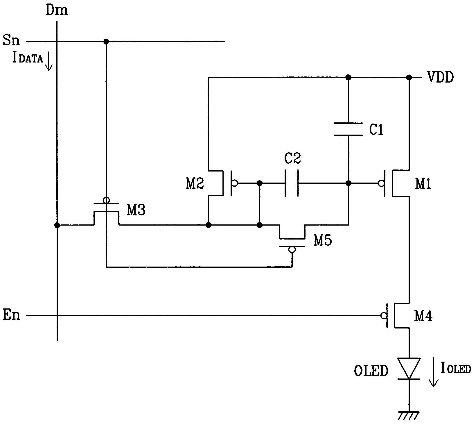
[0041]Next, referring to FIG. 6, an operation of the pixel circuit according to the present invention will be described in detail.

[0042]As shown, in interval T1, transistor M5 is turned on by low-level select signal SEn to couple the gate of transistor M1 and the gate of transistor M2. Transistor M3 is turned on by select signal SEn to have data current IDATA from data line Dm flow to transistor M2. Data current IDATA can be given as Equation 3, and the gate voltage VG3(T1) at transistor M2 in interval T1 is determined from Equation 3. Since the gate of transistor M1 and the gate of transistor M2 are coupled, the gate voltage VG1(T1) at transistor M1 corresponds to the gate voltage VG3(T1) at transistor M2.

[0043]IDATA=12⁢μ2⁢Cox2⁢W2L2⁢(VGS-VTH2)2=12⁢μ2⁢Cox2⁢W2L2⁢(VDD-VG2⁡(T1)-VTH2)Equation⁢⁢3

[0044]where μ2 is electron mobility, Cox2 is oxide capacitance, W2 is a channel width, L2 is a channel length, VTH2 is a threshold voltage of transistor M2, and VDD is a voltage supplied to trans...

second embodiment

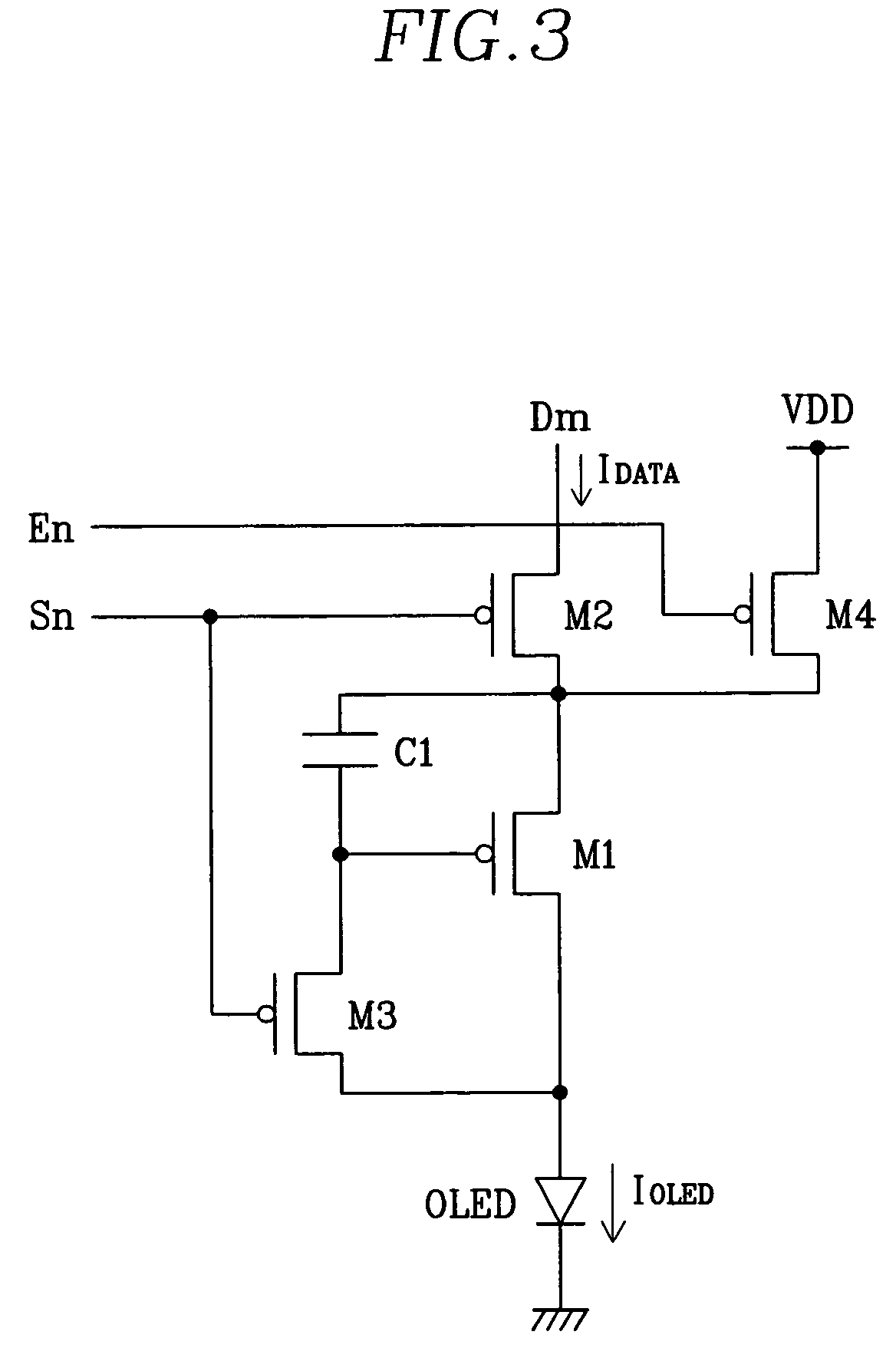
[0058]FIG. 7 shows an equivalent circuit of a pixel circuit according to the present invention, and FIG. 8 shows a driving waveform for driving the pixel circuit of FIG. 7.

[0059]As shown in FIG. 7, the pixel circuit according to the second embodiment further includes scan line Cn in the pixel circuit of FIG. 5. Transistor M5 has a gate coupled to scan line Cn, and couples the gate of transistor M1 to the gate of transistor M2 in response to control signal CSn from scan line Cn.

[0060]Referring to FIG. 8, since turn-on and turn-off timing problem of transistors M3 and M5 can occur in the first embodiment, control signal CSn is set to be low-level prior to select signal SEn. In this instance, a delayed signal of control signal CSn can be used as a select signal SEn.

[0061]In detail, transistor M5 is previously turned on by control signal CSn to couple the gate of transistor M1 and the gate of transistor M2, and transistor M3 is turned on by select signal SEn to transmit data current IDA...


PUM


Abstract

A light emitting display. A first capacitor is coupled between a gate of a first transistor and a power supply voltage. The gate thereof is coupled to a gate of a second transistor, and a data current from a data line is transmitted to the second transistor to set the gate voltages of the first and second transistors as a first voltage. A second capacitor is formed between the gates of the first and second transistors, and the data current from the data line is intercepted. Here, the first capacitor stores a second voltage by coupling of the first and second capacitors. A driving current output from the first transistor is transmitted to a light emitting element, corresponding to the second voltage.

Description

CROSS REFERENCE TO RELATED APPLICATION[0001]This application claims priority to and the benefit of Korea Patent Application No. 2003-20434 filed on Apr. 1, 2003 in the Korean Intellectual Property Office, the content of which is incorporated herein by reference.BACKGROUND OF THE INVENTION[0002](a) Field of the Invention[0003]The present invention relates to a light emitting display, a display panel, and a driving method thereof. More specifically, the present invention relates to an organic electroluminescent (EL) display.[0004](b) Description of the Related Art[0005]In general, an organic EL display electrically excites a phosphorous organic compound to emit light, and it voltage- or current-drives N×M organic emitting cells to display images. As shown in FIG. 1, an organic emitting cell includes an anode of indium tin oxide (ITO), an organic thin film, and a cathode layer of metal. The organic thin film has a multi-layer structure including an emitting layer (EML), an electron tra...

Claims


Application Information

Patent Timeline
Patent Type & Authority Patents(United States)
IPC IPC(8): G09G3/32H01L51/50G09G3/20G09G3/30
CPCG09G3/3241G09G2300/0819G09G2300/0852G09G2320/043G09G2310/0262G09G2320/0252G09G2300/0861G09G3/30
Inventor KWON, OH-KYONG
Owner SAMSUNG DISPLAY CO LTD
Why Eureka
Try Eureka