Solid state image pickup device

a solid-state image and pickup device technology, applied in the direction of printers, optical radiation measurement, camera focusing arrangement, etc., can solve the problems of poor planarization precision, lowered precision of chemical mechanical polishing (cmp) planarization process among cmos manufacture processes, irregular densities of wiring patterns, etc., to improve the accuracy of photometry and range finding, reduce and suppress the incidence of stray ligh

Inactive Publication Date: 2007-01-16
CANON KK
View PDF8 Cites 29 Cited by
  • Summary
  • Abstract
  • Description
  • Claims
  • Application Information

AI Technical Summary

Benefits of technology

[0012]According to the invention, crosstalks to be caused by charge diffusion between the photometry photoelectric conversion elements (AE sensor) and range finding photoelectric conversion elements (AF sensor) can be reduced by electrically separating the second semiconductor region such as a well in which the photometry photoelectric conversion elements (AE sensor) are formed from the third semiconductor region such as a well in which the range finding photoelectric conversion elements (AF sensor) are formed. It is therefore possible to improve the precision of photometry and range finding. By disposing a light shielding layer on the separation region, incidence of stray light can be suppressed. Since crosstalks by stray light can be reduced, the precision of photometry and range finding can be

Problems solved by technology

Stray light indicated by a straight arrow and incident upon photodiodes results in crosstalks.
If the densities of wiring patterns are irregular in the layout of a solid state image pickup device, there occurs a problem of a lowered precision of a chem

Method used


Image

  • Solid state image pickup device
  • Solid state image pickup device
  • Solid state image pickup device

Examples


first embodiment

(First Embodiment)

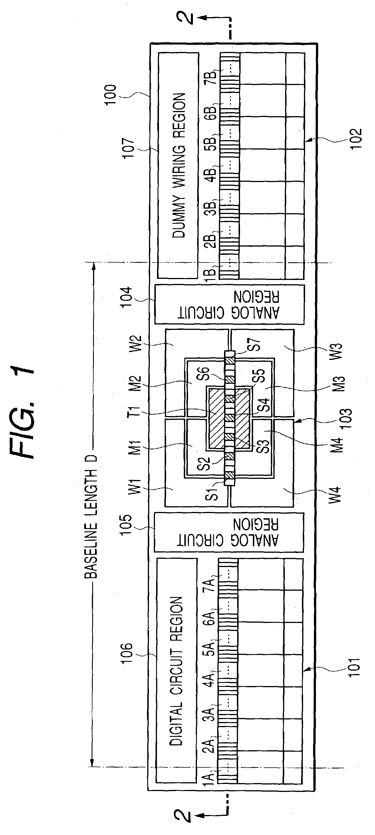
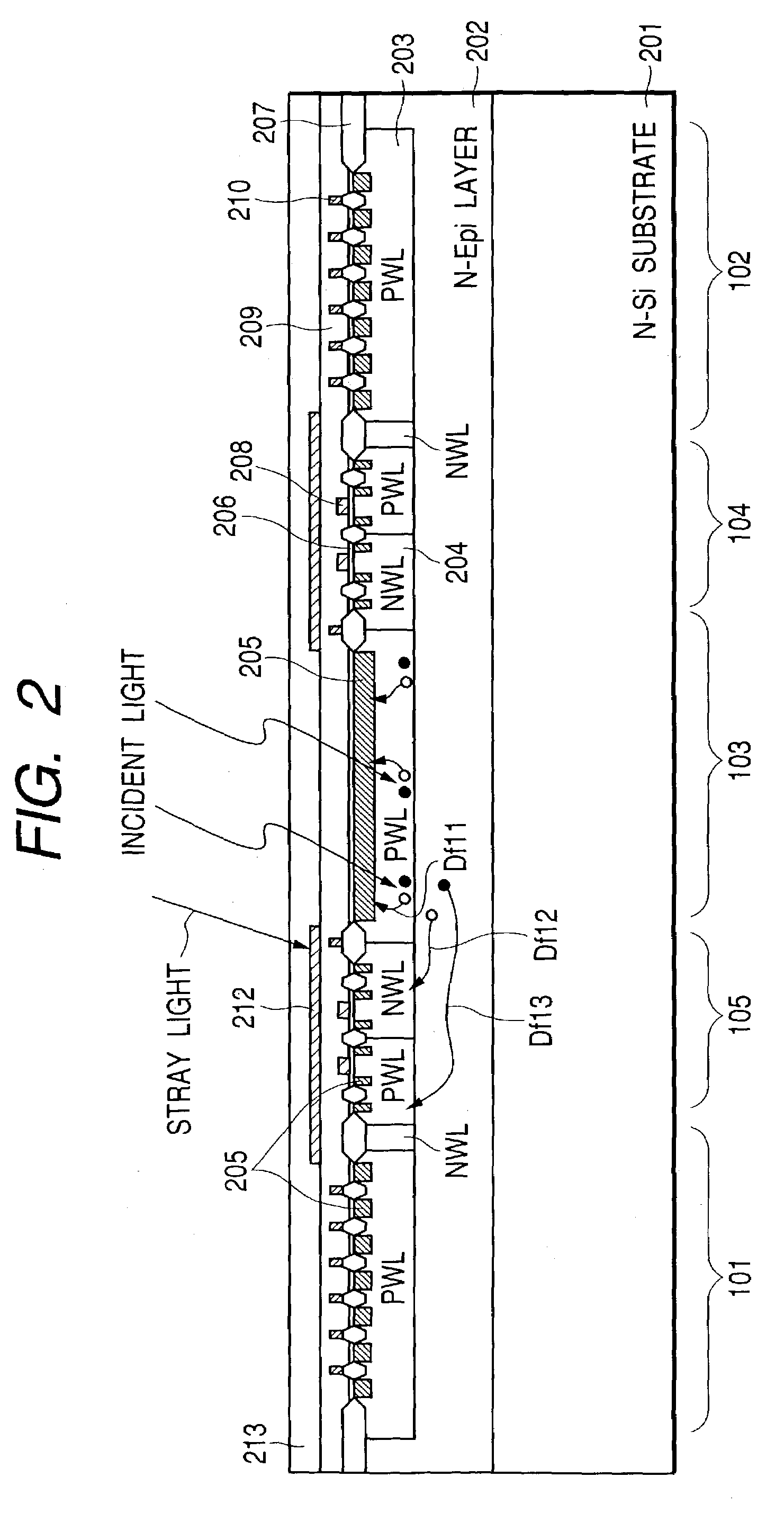
[0028]FIG. 1 is a diagram showing a plan layout of a solid state image pickup device according to a first embodiment of the invention. FIG. 2 is a cross sectional view of the solid state image pickup device taken along line 2—2 in FIG. 1. For the purposes of simplicity, the number of photodiodes of AF and AE sensors drawn in FIG. 1 is reduced. In the first embodiment, the solid state image pickup device is manufactured by using an n-type Si substrate and CMOS processes for a twin well structure of PWL and NWL.

[0029]In FIGS. 1 and 2, reference numeral 100 represents a Si semiconductor substrate (corresponding to an n-type Si substrate 201 shown in FIG. 2), 101 and 102 represent AF sensor regions, 103 represents an AE sensor region, 104 and 105 represent analog circuit regions, 106 represents a digital circuit region and 107 represents a dummy wiring pattern region. In FIG. 2, reference numeral 201 represents the n-type Si substrate, 202 represents an n-type epitaxia...

second embodiment

(Second Embodiment)

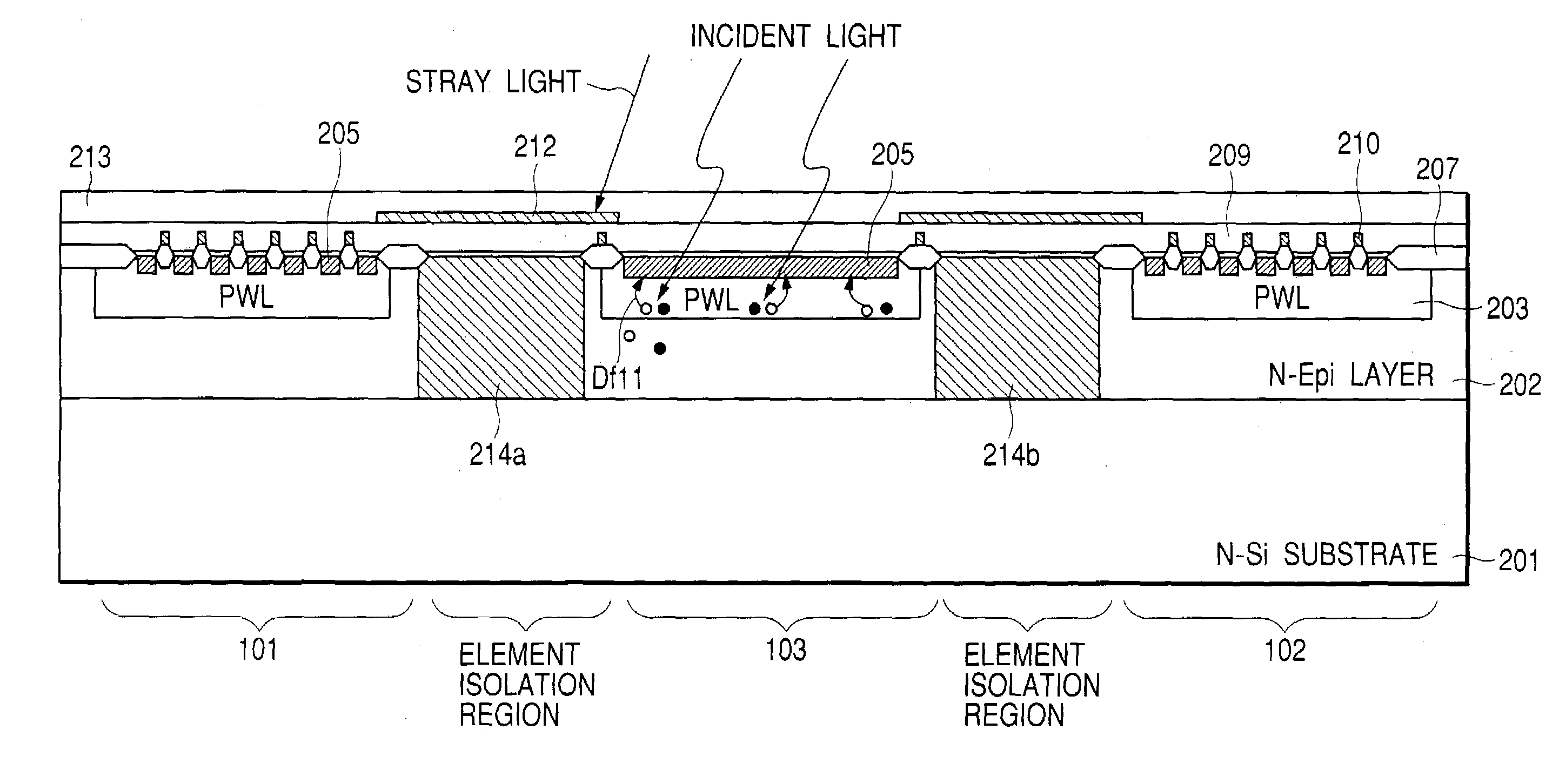
[0051]FIG. 6 is a diagram showing a plan layout of a solid state image pickup device according to a second embodiment of the invention, and FIG. 7 is a cross sectional view of the solid state image pickup device of the second embodiment. In FIGS. 6 and 7, reference symbol 100a represents an Si semiconductor substrate, 214a and 214b represent n+-type diffusion regions, and 212a and 212b represent light shielding layers. Reference numeral 215 represents an AF sensor circuit in the AF sensor region 101. In this embodiment, high impurity concentration regions (n-type element isolation regions) 214a and 214b of the same conductivity type as that of the substrate are disposed between the AF sensor regions 101 and 102 and the AE sensor region 103 in order to further reduce crosstalks between the AE and AF sensor regions. The crosstalk reduction effects of the second embodiment are better than those of the first embodiment. However, analog circuits are required to be form...

third embodiment

(Third Embodiment)

[0052]FIG. 8 is a diagram showing a plan layout of a solid state image pickup device according to a third embodiment of the invention. In FIG. 8, reference numeral 215 represents an n+-type buried layer. This embodiment is characterized in that the wells of the AE sensor region 103 and AF sensor regions 101 and 102 are perfectly separated by the n+-type high impurity concentration layer 214 and n+-type buried layer 215. Although the burying process is necessary, this embodiment is effective for reducing crosstalks by all means.

[0053]As shown in FIG. 9, instead of an n-type Si substrate, a p-type substrate may also be used with similar expected effects.


PUM


Abstract

A solid state image pickup device is provided which can reduce crosstalks between range finding photoelectric conversion elements (AF sensor) and photometry photoelectric conversion elements (AE sensor). The solid state image pickup device has an n-type epitaxial semiconductor region, a p-type first well region formed in the semiconductor region, a p-type second well region formed in the semiconductor region and electrically separated from the first well, an n-type first impurity doped region formed in the first well region and an n-type second impurity doped region formed in the second well, wherein a photometry photoelectric conversion element is formed by using the p-type first well region and n-type first impurity doped region, and a range finding photoelectric element is formed by using the p-type second well region and n-type impurity doped region.

Description

BACKGROUND OF THE INVENTION[0001]1. Field of the Invention[0002]The present invention relates to a solid state image pickup device suitable for use as an automatic focussing solid state image pickup device with a photometry function, particularly as a compact camera automatic focussing sensor of a phase difference detection and external photometry type.[0003]2. Related Background Art[0004]A range finding (automatic focussing, AF) sensor with a photometry (automatic exposure, AE) function for a conventional lens-shutter compact camera has been realized as a solid state image pickup device as disclosed, for example, in U.S. Pat. No. 5,302,997. A schematic plan layout of this solid state image pickup device is shown in FIG. 11. Referring to FIG. 11, an AE sensor array 30 is constituted of an AE center segment 32, AE inner segments 34A, 34B, 34C and 34D and AE outer segments 36A, 36B, 36C and 36D. The solid state image pickup device has also AF sensor arrays (linear sensor arrays) 40 an...

Claims


Application Information

Patent Timeline
IPC IPC(8): H04N5/232G03B3/10H01L31/06H01L31/062H04N5/238H04N5/335G01J1/02G03B13/00H01L27/14H01L27/146H01L31/11H04N5/228H04N5/359H04N5/374
CPCH01L31/11H01L27/14643
Inventor TAKAHASHI, HIDEKAZU
Owner CANON KK
Why Eureka
Try Eureka