Transistor gate and local interconnect

Inactive Publication Date: 2007-02-13
MICRON TECH INC
View PDF28 Cites 0 Cited by
  • Summary
  • Abstract
  • Description
  • Claims
  • Application Information

AI Technical Summary

Benefits of technology

[0012]The aforementioned needs are satisfied by the integrated circuit of the present invention. According to one aspect of the invention, the integrated circuit comprises a semiconductor substrate and a first electrical structure formed in the semiconductor substrate. The integrated circuit further comprises a gate stack formed on the semiconductor substrate, the gate stack having at least one conductive layer and a source layer positioned on the conductive layer. The integrated circuit further comprises a local interconnect interconnecting the conductive layer of the gate stack to the first electrical structure. In particular, the local interconnect is attached to the gate stack at an exhumed surface adjacent the layer of source material. Moreover, the local interconnect includes a conductive material to provide a low resistance contact with the first electrical structure formed in the semiconductor substrate. The source layer provides transforming atoms to the material used to form the local interconnect during formation such that the density of dopant atoms in the material used to form the local interconnect during formation is sufficient to substantially prevent undercutting of the local interconnect at the connection to the gate stack.
[0015]In one embodiment, the transforming atoms are comprised of silicon such that the local interconnect forms a silicide material at the exhumed contact. In this embodiment, the method of forming a local interconnect further comprises removing the excess refractory material such that the refractory silicide contact is substantially preserved. In this embodiment, the source material provides sufficient silicon atoms to the refractory material during transformation of the refractory material to reduce undercutting of the refractory silicide contact at the exposed surface of the source material.

Problems solved by technology

While silicides are very versatile as materials for forming interconnecting structures in integrated circuits, in some applications the suicides may poorly interconnect to particular semiconductor devices.
For example, with some exhumed contact structures, the processing steps may result in the interconnect structure being undercut at an exposed region adjacent the exhumed contact which can result in either a higher resistance contact or an open contact which may be inadequate for a particular application.
However, FIG. 1 illustrates a common problem associated with this kind of interconnect.
Thus, circuit performance may be compromised and production yields may be decreased.
Moreover, such problematic local interconnects may limit the extent of selective wet cleans, which could impede the development of increasingly reduced circuit dimensions.

Method used


Image

  • Transistor gate and local interconnect
  • Transistor gate and local interconnect
  • Transistor gate and local interconnect

Examples


Embodiment Construction

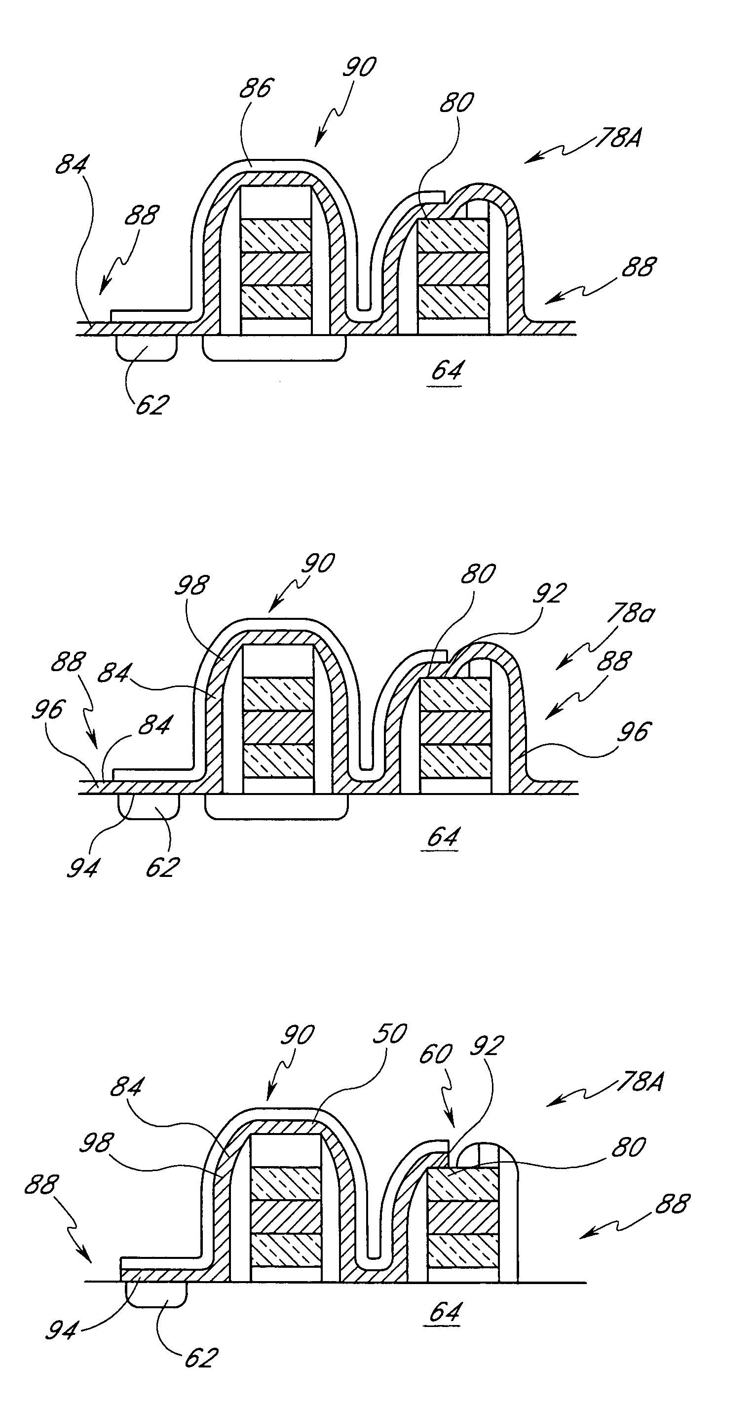
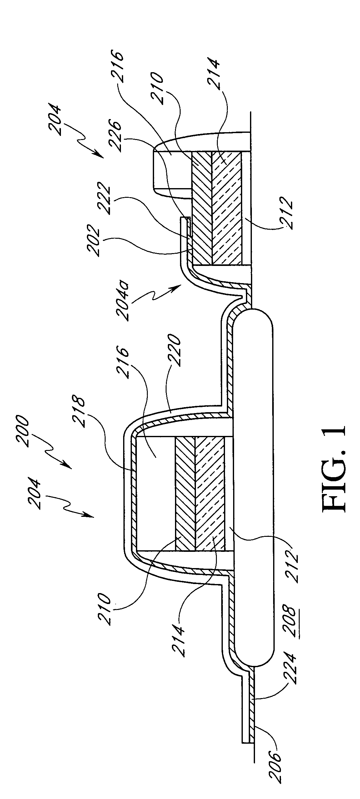
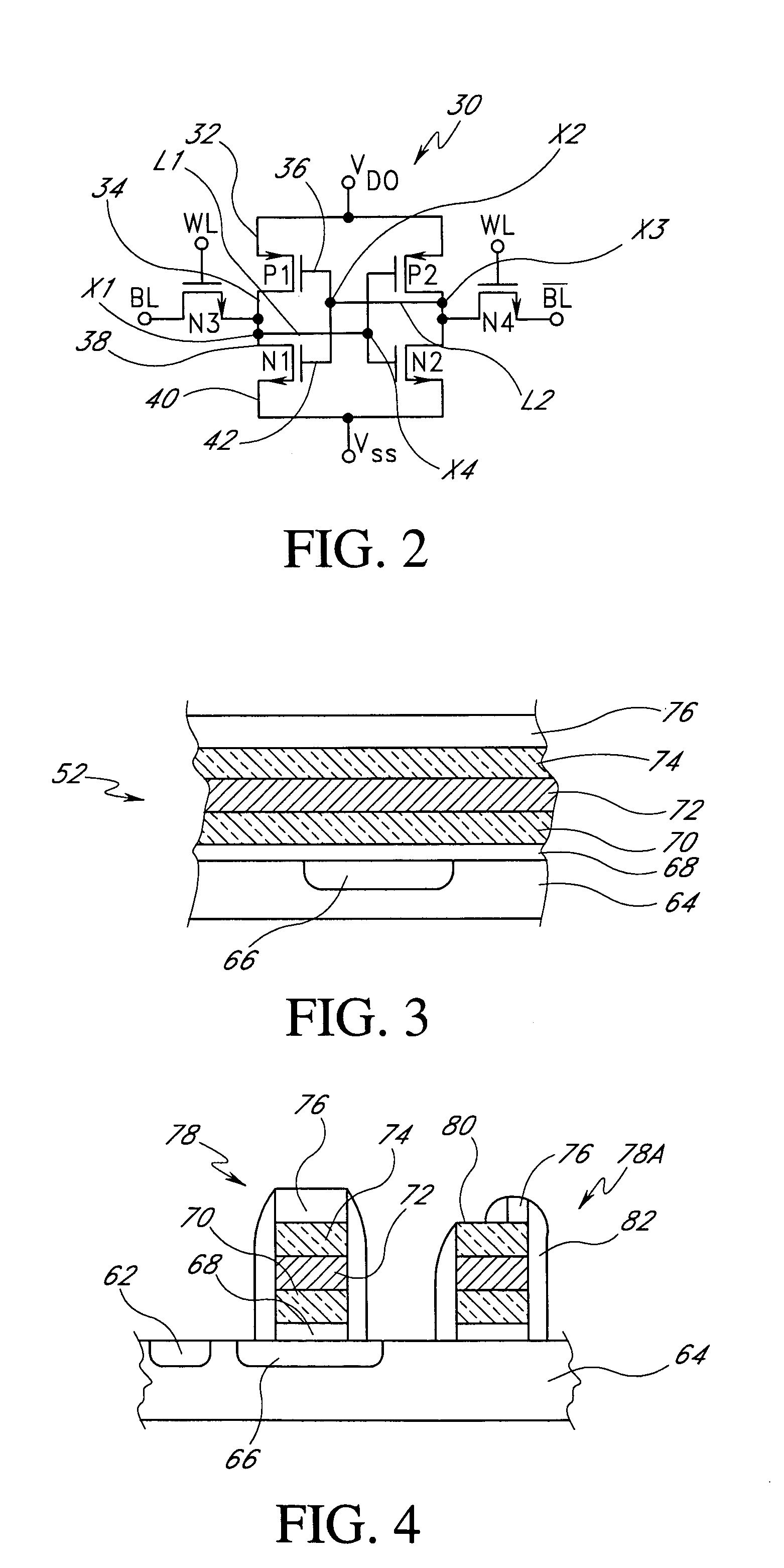
[0020]Reference will now be made to the drawings wherein like numerals refer to like parts throughout. As is understood in the art, interconnects are used to interconnect various circuit components of semiconductor devices. To provide context and background, a circuit diagram of a typical integrated circuit formed on a semiconductor substrate is initially described in connection with FIG. 2. The circuit illustrated in FIG. 2 is simply one example of a typical circuit formed on an integrated circuit that requires the use of low resistance local interconnects. It will be appreciated from the following discussion that local interconnects are used in many different types of integrated circuits including SRAM, DRAM and other non-memory circuits and, as such, the present invention should not be limited to only the circuit of FIG. 2. The process by which the interconnect of the illustrated embodiment will be described in greater detail below in connection with FIGS. 3–7.

[0021]As shown in F...


PUM


Abstract

A method of forming a local interconnect for a semiconductor integrated circuit, the local interconnect comprising a refractory silicide contact having a substantially small sheet resistance formed at an exhumed surface of a gate stack, wherein the local interconnect electrically couples a gate electrode of the gate stack with an active region of the semiconductor substrate. The method of forming the local interconnect comprises depositing a gate oxide layer over the substrate, a first polysilicon layer over the gate oxide layer, a laterally conducting layer over the polysilicon layer, a second polysilicon layer over the laterally conducting layer, and an insulating layer over the second polysilicon layer. The intermediate structure is then etched so as to form a plurality of gate stacks. A surface of the second polysilicon layer of a gate stack is exhumed so as to allow subsequent formation of the refractory silicide contact at the exhumed surface. A plurality of spacers are formed along the vertical surfaces of the gate stacks and the substrate is selectively doped so as to form active regions within the substrate. A layer of titanium is deposited over the substrate and a silicon source and / or hardmask material layer is deposited over the titanium layer so as to extend between the gate electrode and the active region of the silicon. The mask layer is then patterned in an etching process so that the mask layer defines the extent of the local interconnect structure. The intermediate structure is then exposed to a high temperature N2 / NH3 ambient which induces the formation of refractory silicide contacts at the exhumed surface of the polysilicon layer of the gate stack and at the active region of the substrate as well as the formation of refractory nitride (TiN) at the exposed portions of the titanium layer. A selective wet etch follows which removes the exposed unreacted titanium and exposed titanium nitride and leaves behind the local interconnect.

Description

RELATED APPLICATIONS[0001]This application is a divisional of U.S. patent application Ser. No. 09 / 360,703 filed Jul. 26, 1999 and issued as U.S. Pat. No. 6,630,718 Oct. 7, 2003 which is incorporated herein in its entirety by reference.BACKGROUND OF THE INVENTION[0002]1. Field of the Invention[0003]The present invention relates to semiconductor integrated circuit fabrication, devices and methods, and, in particular, is directed toward the method of forming a unique silicide local interconnect structure that extends from an exhumed gate electrode.[0004]2. Description of the Related Art[0005]As is well known in the semiconductor processing industry, refractory silicides are often used to form local interconnects between circuit nodes in a semiconductor integrated circuit. In particular, when a refractory metal, for example titanium (Ti), is deposited flushly adjacent a silicon material and exposed to a sufficiently high temperature, the refractory metal will react with the silicon mate...

Claims


Application Information

Patent Timeline
IPC IPC(8): H01L21/336H01L21/3205H01L21/44H01L21/768H01L21/8234H01L23/485H01L31/113
CPCH01L21/76895H01L21/823475H01L23/485H01L2924/0002H01L2924/00
Inventor TRIVEDI, JIGISH D.
Owner MICRON TECH INC
Why Eureka
Try Eureka