Method of forming thin metal films on substrates

a technology of thin metal film and substrate, which is applied in the direction of resistive material coating, heat inorganic powder coating, solid-state devices, etc., can solve the problems of inability to meet the requirements of the application, etc., to achieve convenient forming, high conductivity, and the effect of convenient application

Inactive Publication Date: 2007-02-20
EBARA CORP
View PDF18 Cites 4 Cited by
  • Summary
  • Abstract
  • Description
  • Claims
  • Application Information

AI Technical Summary

Benefits of technology

[0014]It is therefore an object of the present invention to provide a solution containing a metal component for use in inexpensively and easily forming a conductive thin metal film which has a sufficient conductivity and whose thickness can easily be adjusted, and a method of and an apparatus for forming a thin metal film using such a solution.

Problems solved by technology

While the plating technology is inexpensive and technically highly complete, the electrolytic plating process allows films to be grown on only conductive materials, and the electroless plating process is open to environmental pollution as materials contained in the plating solution adversely affect the natural environment and the working and labor environment.
If a thin metal film is formed of a conventional metal paste as interconnections on a ceramic substrate, then the conductivity is limited to a certain level because the thin metal film is rendered conductive by point-to-point contact between metal particles.
The thicker metal film is more expensive to manufacture.
However, available processes of producing ultrafine metal particles are of low productivity.
The processes of producing ultrafine metal particles also disadvantageous in that it is difficult to keep the ultrafine particles in safe storage because once the solvent is evaporated, the particles stick to each other and cannot be reused.

Method used


Image

  • Method of forming thin metal films on substrates
  • Method of forming thin metal films on substrates
  • Method of forming thin metal films on substrates

Examples


Embodiment Construction

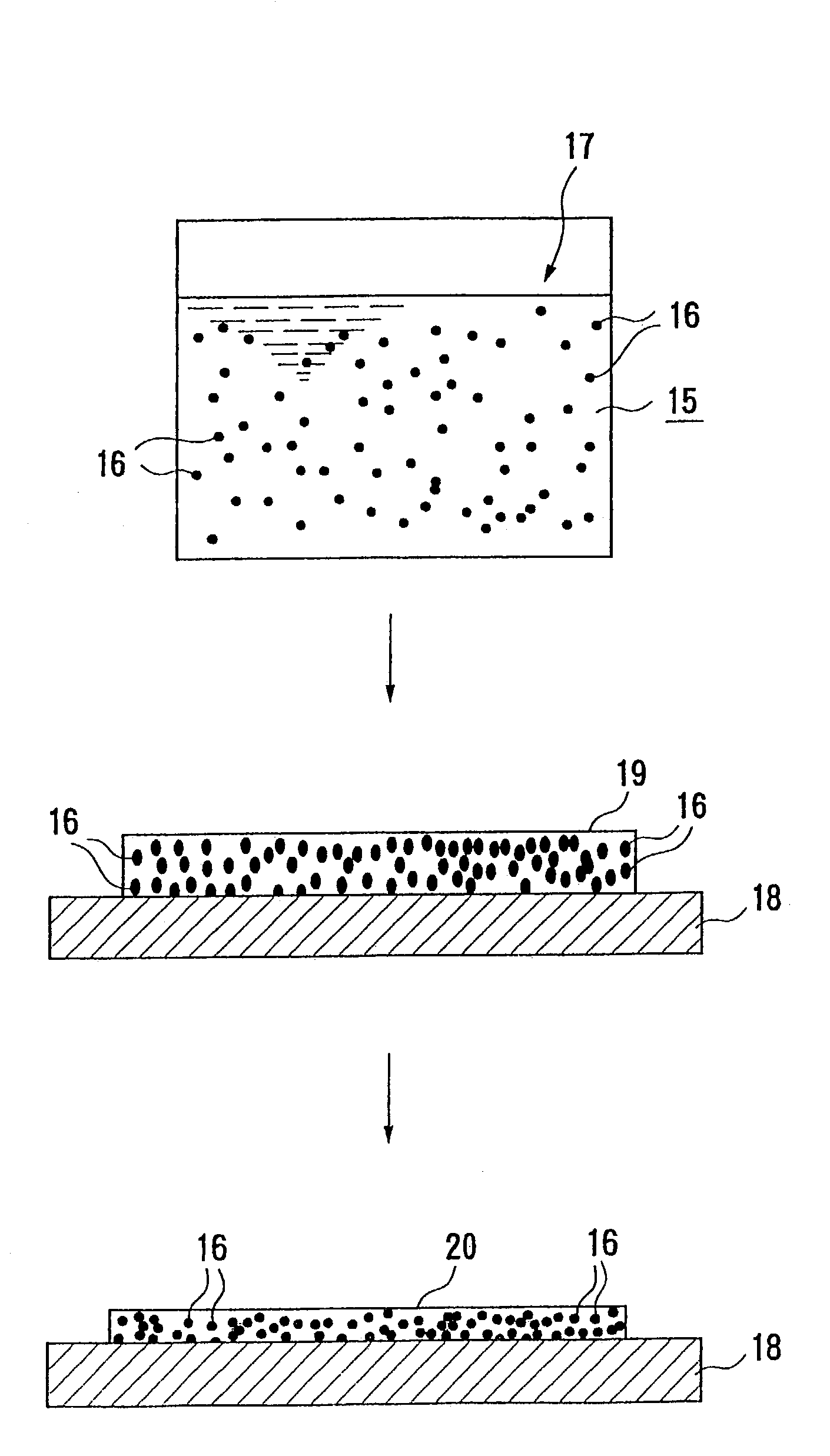
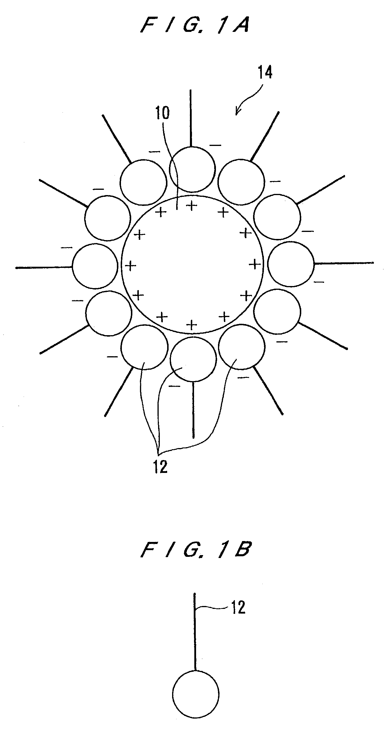
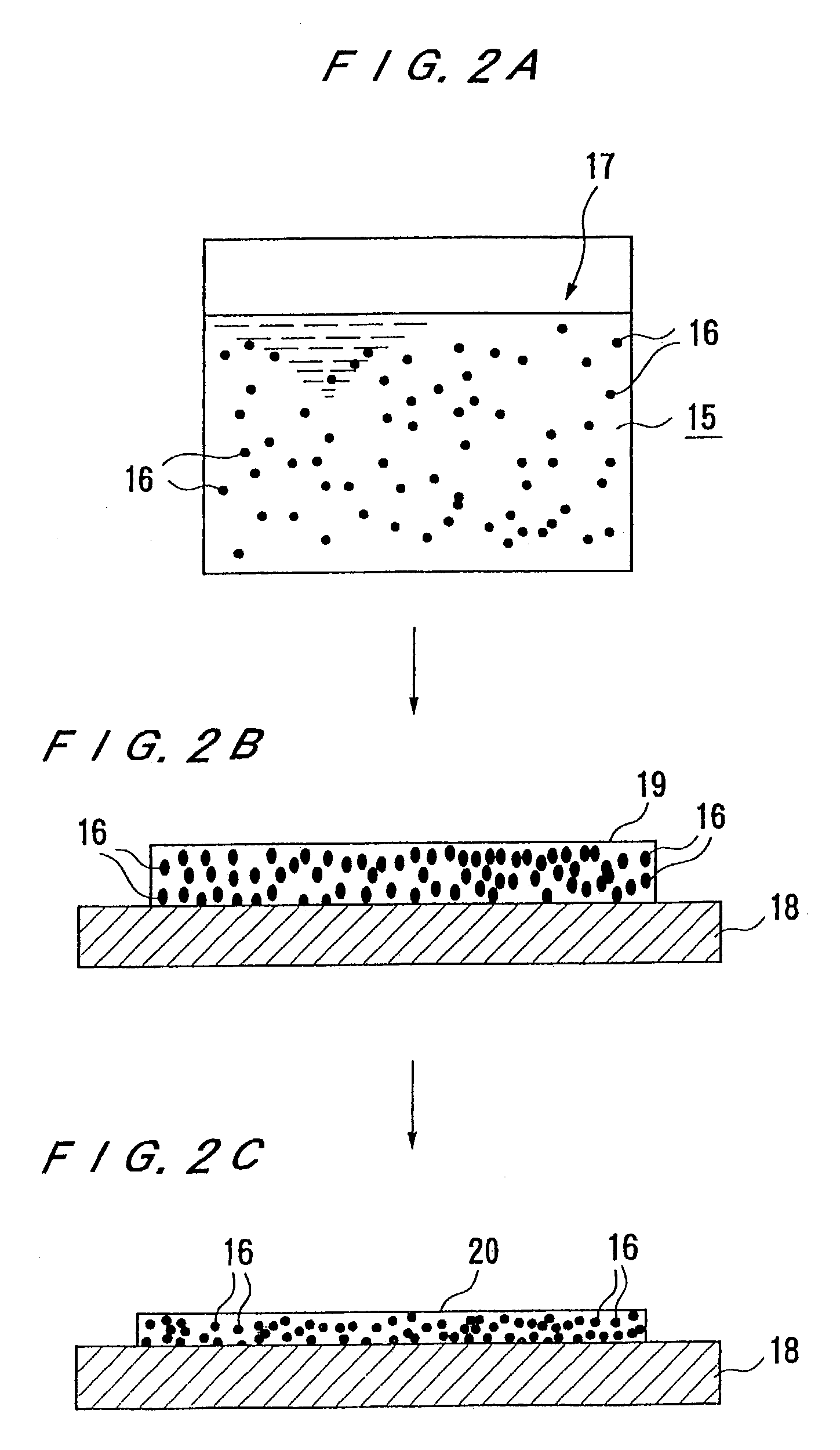
[0083]As shown in FIGS. 1A and 1B, a composite ultrafine metal particle 14 comprising a core 10 substantially made of a metal component and a covering layer 12 made of an organic compound is prepared. The composite ultrafine metal particle 14 is stable because it has the covering layer 12 made of an organic compound, and is less liable to be aggregated in a solvent.

[0084]The composite ultrafine, metal particle 14 is composed of the organic compound and the metal component which derives from a metal salt as a starting material, e.g., a carbonate, a formate, or an acetate. The core 10 is made of the metal component, and surrounded by the covering layer 12 of the ionic organic compound. The organic compound and the metal component are partly or wholly chemically coupled to each other. The composite ultrafine metal particle 14 is highly stable, and stable in a higher metal concentration, unlike the conventional ultrafine particles which are stabilized by being coated with a surface acti...


PUM

PropertyMeasurementUnit
diameteraaaaaaaaaa
weight %aaaaaaaaaa
diameteraaaaaaaaaa

Abstract

A solution containing a metal component of composite ultrafine metal particles each having a core substantially made of metal component and a covering layer made of an organic compound chemically bonded to the core having an average diameter ranging from 1 to 10 nm, uniformly dispersed in a solvent, forms a thin metal film on the surface of a transfer sheet, after which the transfer sheet, after which the transfer sheet is thermally decomposed to transfer the thin metal film to a substrate.

Description

[0001]This is a division of co-pending parent application Ser. No. 09 / 733,084 filed Dec. 11, 2000, now abandoned.BACKGROUND OF THE INVENTION[0002]1. Field of the Invention[0003]The present invention relates to a solution containing a metal component, and a method of and an apparatus for forming a thin metal film, and more particularly to a solution containing a metal component for use in forming a conductive thin metal film on a semiconductor substrate of silicon or the like, and a method of and an apparatus for forming a thin metal film using such a solution, and a method of and an apparatus for forming a thin metal film in embedding a conductive metal such as copper (Cu) or the like in minute interconnection recesses defined in the surface of a substrate of silicon or the like thereby forming interconnections.[0004]2. Description of the Related Art[0005]Aluminum or aluminum alloys are generally used as metal materials for forming interconnection circuits on semiconductor substrate...

Claims


Application Information

Patent Timeline
Patent Type & Authority Patents(United States)
IPC IPC(8): B05D5/12B05D3/02H01L21/20B22F1/052B22F1/054B22F1/0545B22F1/10B22F1/102C23C4/12H01L21/00H01L21/288H01L21/768H01L23/532
CPCB22F1/0014B22F1/0018H01L23/5328B22F1/0022B22F1/0059B22F1/0062B82Y30/00C23C4/121C23C24/08C23C26/00H01L21/288H01L21/6715H01L21/76877H01L21/76882H01L23/53228H01L23/53238B22F2998/00H01L2924/0002C23C4/123B22F1/0545B22F1/052B22F1/102B22F1/054B22F1/10H01L2924/00H01L21/20
Inventor FUKUNAGA, AKIRANAGASAWA, HIROSHIKATO, TAKAO
Owner EBARA CORP
Why Eureka
Try Eureka