Wireless no-touch testing of integrated circuits

a technology of integrated circuits and testing methods, applied in the direction of error detection/correction, instruments, semiconductor/solid-state device testing/measurement, etc., can solve the problems of increasing test costs, increasing the cost of integrated circuit testing, and continuing to fall the cost of integrated circuit fabrication, so as to increase the speed of loading the chain and reduce the impact of cos

Active Publication Date: 2007-02-20
ADVANTEST CORP
View PDF4 Cites 51 Cited by
  • Summary
  • Abstract
  • Description
  • Claims
  • Application Information

AI Technical Summary

Benefits of technology

[0015]The present invention is a method and apparatus for testing integrated circuits over a wireless communication channel that minimizes the required integrated circuit test pin / pad count, decreases test time, and is economical. The technique of the invention allows testing of an integrated circuit with minimal physical probe contact (i.e., without requiring the use of a dedicated integrated circuit tester), and further allows testing during multiple phases of the life cycle of the integrated circuit. In addition, the invention may be adapted to allow testing of multiple integrated circuits of the same design in parallel.
[0019]In addition, standard wireless Internet protocols such as IEEE 802.11 Wireless WLAN and 801.15 Wireless WPAN protocols such as Bluetooth allow communication with multiple wireless devices at the same time. Accordingly, the test station can be configured to handshake with the wireless IP core of multiple integrated circuits under test and then begin sending and receiving test data to all the devices simultaneously. This technique enables a massively parallel testing approach using common PC hardware, resulting in immediate cost-reduction impacts.
[0020]The present invention may also be used to test integrated circuits that are designed for CCT. Test data throughput is typically limited by internal serial scan chain load / unload frequency of about 20 MHz. Standard wireless IP protocols can run at significantly higher speeds, and transport data in packaged units called frames containing varying numbers of bytes, words, or blocks. The data is recovered frame by frame; thus each frame is released from the wireless protocol stack (e.g., TCP / IP) only when the entire frame is present, or essentially in parallel. Accordingly, each bit in the bytes, words, or blocks of the frame can be treated as a separate channel and assigned to drive a separate scan chain or other internal port in the device. Accordingly, multiple scan chains can be loaded in parallel, thereby increasing the speed of loading the chains, and ultimately decreasing the time for testing the device. Similarly, data from multiple output ports can be recovered in parallel, formatted into frames, and returned to the test station via standard IP protocols.

Problems solved by technology

However, as the cost of integrated circuit fabrication continues to fall, the cost of integrated circuit testing has increased.
One reason for increasing test costs is based on the increasing ratio of number of transistors to number of implementable pads on an integrated circuit.
The increasing trend to integrate greater capability into IC's, resulting in embedded complexities, has significantly reduced the effectiveness of the present in-circuit testing methods at the board level via a “bed of nails” interface.
Due to the physical limitations of external test probes in terms of required size and spacing, the number of external pads is likely to decrease rather than increase, and will certainly not keep up with the rate of increase in number of integrated circuit transistors.
However, because data must be applied serially to the integrated circuit, it increases test time, and therefore test cost.
However, in each of the above techniques, the cost of test is still high because currently, expensive “bed-of-nails” testers are still used to probe the test access points on the integrated circuits under test.
DFT techniques suffer from several common limitations.
One typical difficulty is that DFT often requires a large amount of memory for storing test data.
While BIST overcomes this problem by including test pattern generators for generating predictable patterns of test data without storing it, standard BIST techniques are typically covered by BIST intellectual property, which can be expensive to purchase and uses precious space on the chip.

Method used


Image

  • Wireless no-touch testing of integrated circuits
  • Wireless no-touch testing of integrated circuits
  • Wireless no-touch testing of integrated circuits

Examples


Embodiment Construction

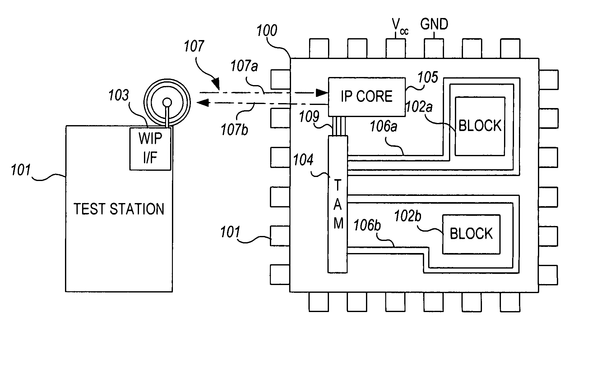
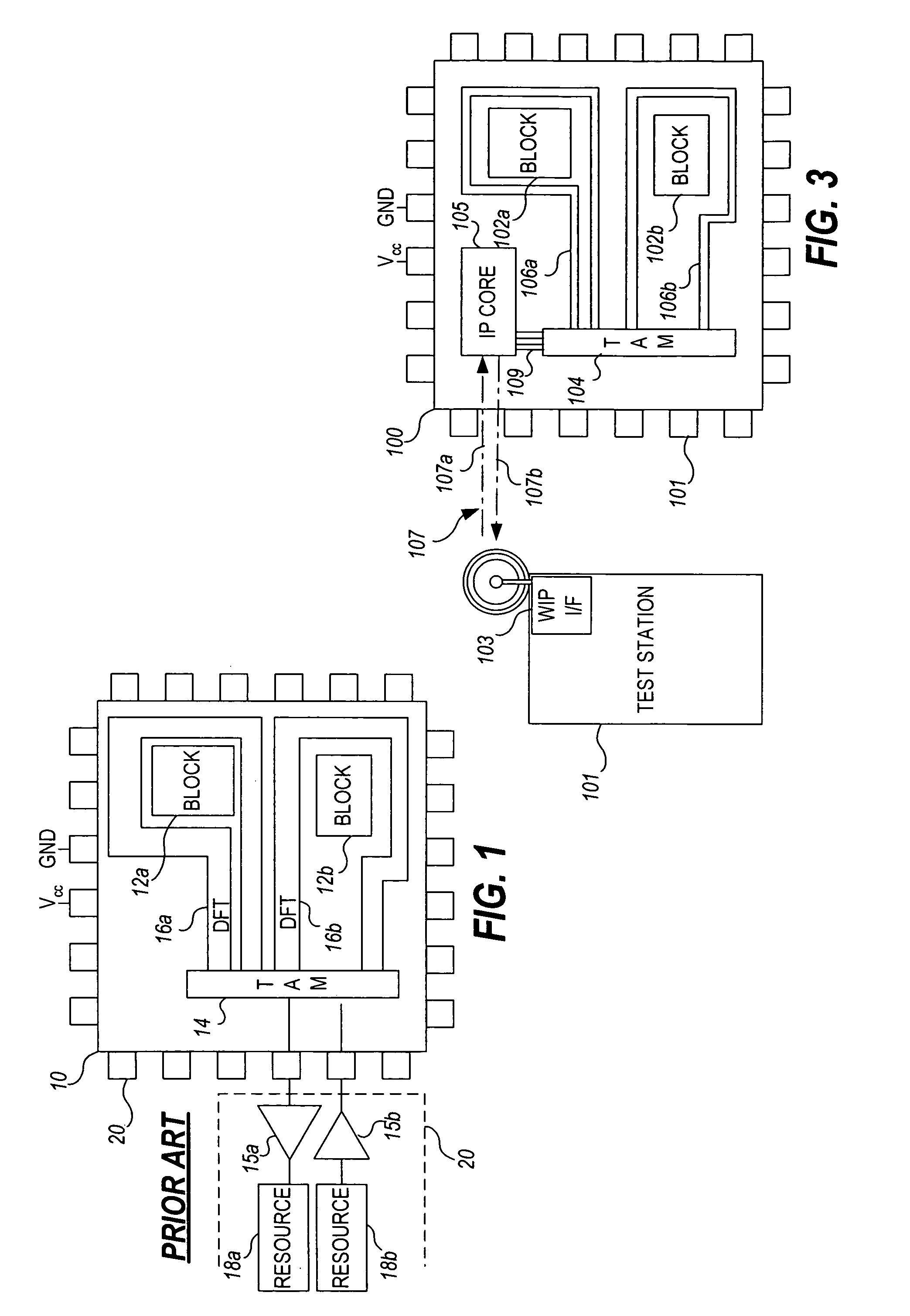
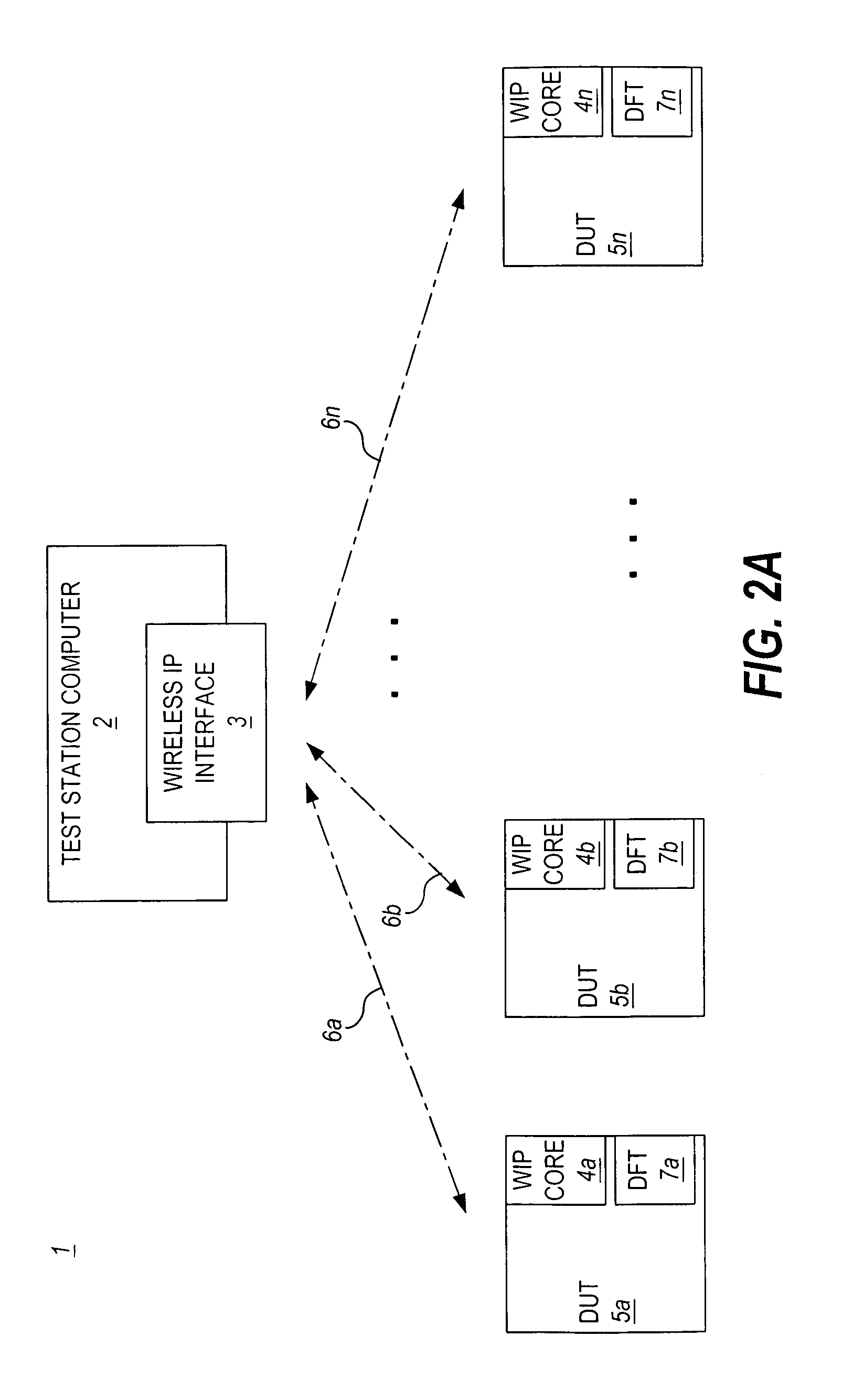
[0029]Turning now to the drawings, FIG. 2A is a high-level system diagram, and FIG. 2B is an operational flowchart, of an integrated circuit test system 1 illustrating the general concept of the invention. As illustrated, according to the present invention, a single test station computer 2 equipped with a wireless internet protocol interface 1 is configured to communicate with one or more devices under test (DUTs) 5a, 5b, . . . , 5n equipped with wireless IP cores 4a, 4b, . . . , 4n over a wireless IP connection 6a, 6b, 6c. The wireless IP cores 4a, 4b, . . . , 4n are connected to or are connectable to DFT structures 7a, 7b, . . . , 7n that are configured to test various functional blocks (not shown) within the respective DUTs 5a, 5b, . . . , 5n. The DUTs 5a, 5b, 5n may be integrated circuit wafers, packaged integrated chips, printed circuit boards, etc., as long as they include some form of Design-For-Test functionality that requires digital test data.

[0030]The test station 2 sends...


PUM


Abstract

A wireless integrated circuit test method and system is presented. The invention allows testing of one or more integrated circuits configured with a wireless interface and a test access mechanism which controls input of test data received over a wireless connection from a test station to test structures which test functional blocks on the integrated circuit. Via the wireless connection, multiple integrated circuits or similarly equipped devices under test can be tested simultaneously. The invention also enables concurrent testing of independently testable functional blocks on any given integrated circuit under test.

Description

BACKGROUND OF THE INVENTION[0001]Integrated circuit testing is critical at both the design level to confirm proper operation of a given design and at the manufacturing level for ensuring a given chip meets all manufacturing specifications prior to shipment. However, as the cost of integrated circuit fabrication continues to fall, the cost of integrated circuit testing has increased. One reason for increasing test costs is based on the increasing ratio of number of transistors to number of implementable pads on an integrated circuit. For example, the ratio of the number of transistors to number of pads increased from 2,500 in 1990 to 300,000 in 2001. Undoubtedly, this trend for smaller and smaller integrated circuits with increasing transistor density will continue. The increasing trend to integrate greater capability into IC's, resulting in embedded complexities, has significantly reduced the effectiveness of the present in-circuit testing methods at the board level via a “bed of na...

Claims


Application Information

Patent Timeline
Patent Type & Authority Patents(United States)
IPC IPC(8): G01R31/28G06F11/00G01R31/302G01R31/303G01R31/3185G01R31/319G11C29/00H01L21/66H01L21/822H01L27/04
CPCG01R31/2886G01R31/3025G01R31/318572G01R31/31905H01L2924/0002H01L2924/00
Inventor HILDEBRANT, ANDREW S.
Owner ADVANTEST CORP
Why Eureka
Try Eureka