Epitaxial and polycrystalline growth of Si1-x-yGexCy and Si1-yCy alloy layers on Si by UHV-CVD

a technology which is applied in the field of epitaxial and polycrystalline growth of si, can solve the problem that no prior art technology can achieve the effect of achieving the effect of ycy and si1-ycy alloy layers on si

Inactive Publication Date: 2007-02-27
GLOBALFOUNDRIES INC
View PDF14 Cites 14 Cited by
  • Summary
  • Abstract
  • Description
  • Claims
  • Application Information

AI Technical Summary

Benefits of technology

[0011]It is a further object of the present invention to provide an apparatus and method for enabling low temperature epitaxy of silicon carbon layers having very low concentrations of oxygen contaminants in the SiC layers, preferably less than 1×10¹⁷ O atoms cm−3.
[0025]It is a further object of the present invention to provide a method and apparatus for performing in-situ p- or n-type doping of polycrystalline silicon germanium carbon layers which can withstand furnace anneals to temperatures of 850° C. and rapid thermal anneal temperatures to 1000° C.

Problems solved by technology

Furthermore, the fabrication of very thin epitaxial layers of silicon carbon or silicon germanium carbon having abrupt transitions of several atomic widths in carbon concentration between adjacent single crystal layers, which cannot be achieved by any prior art techniques, is provided.

Method used


Image

  • Epitaxial and polycrystalline growth of Si1-x-yGexCy and Si1-yCy alloy layers on Si by UHV-CVD
  • Epitaxial and polycrystalline growth of Si1-x-yGexCy and Si1-yCy alloy layers on Si by UHV-CVD
  • Epitaxial and polycrystalline growth of Si1-x-yGexCy and Si1-yCy alloy layers on Si by UHV-CVD

Examples


Embodiment Construction

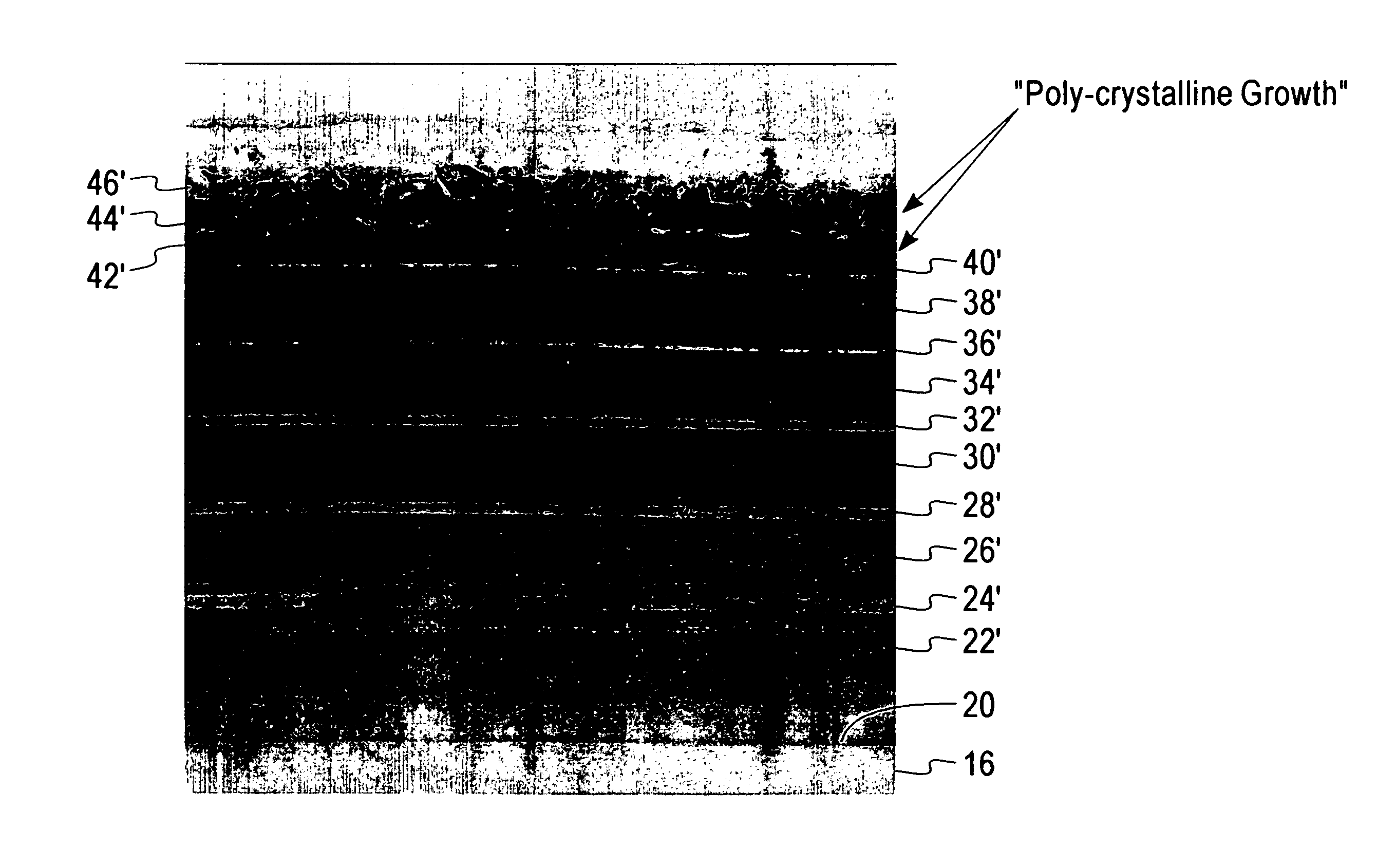
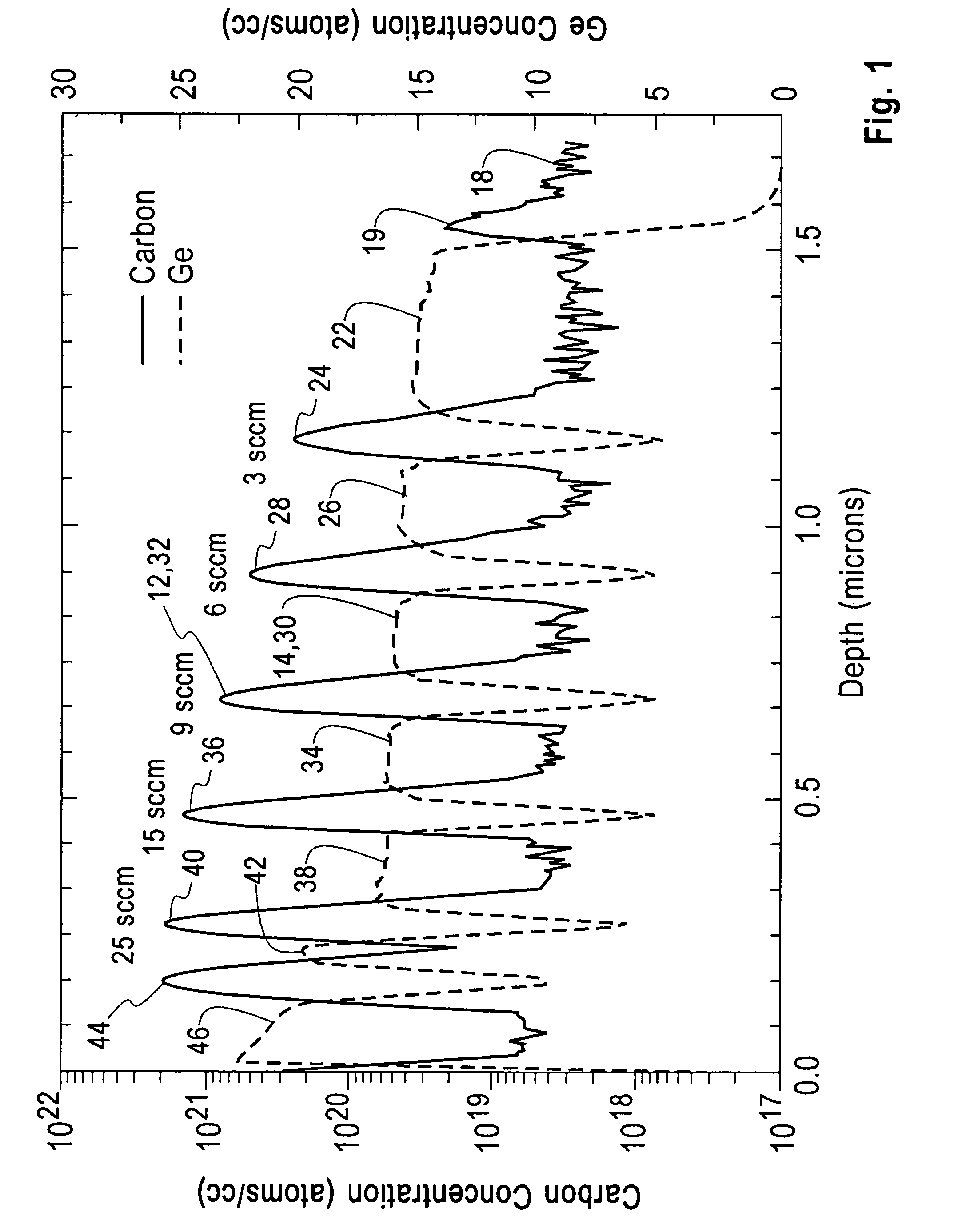
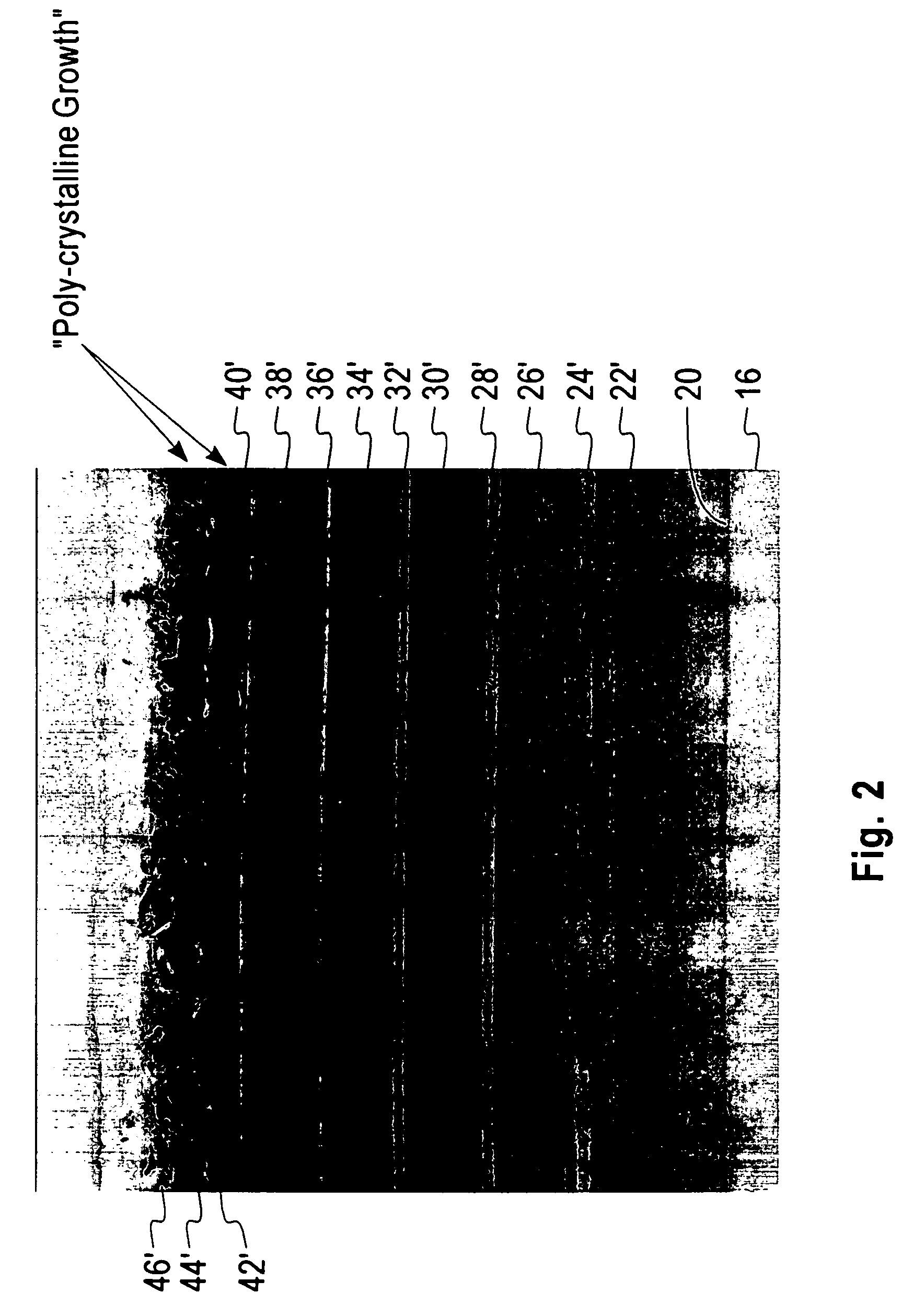
[0038]This invention is an apparatus and process for depositing epitaxial single crystal silicon carbon and silicon germanium carbon layers of a desired thickness on a silicon containing substrate, and in particular to provide a process whereby single crystal silicon carbon alloy layers can be epitaxially deposited on a multitude of substrates. These silicon carbon and silicon germanium carbon alloy films are of high crystallographic perfection suitable for device applications and furthermore, can be in-situ doped to any desired levels without any oxygen contamination which is detrimental to device performances. The present invention of growing silicon carbon and silicon germanium carbon films,. i.e. SiC, SiC:B, SiC:P, SiGeC, SiGeC:B, SiGeC:P utilizes the UHV-CVD technique for growing epitaxial Si and SiGe films on a silicon containing substrate. For a description of the UHV-CVD growth technique, reference is made to U.S. Pat. No. 5,298,452 which issued Mar. 29, 1994 to B. S. Meyers...


PUM

PropertyMeasurementUnit
frequency performanceaaaaaaaaaa
base widthaaaaaaaaaa

Abstract

A method and apparatus for depositing single crystal, epitaxial films of silicon carbon and silicon germanium carbon on a plurality of substrates in a hot wall, isothermal UHV-CVD system is described. In particular, a multiple wafer low temperature growth technique in the range from 350° C. to 750° C. is described for incorporating carbon epitaxially in Si and SiGe films with very abrupt and well defined junctions, but without any associated oxygen background contamination. Preferably, these epitakial SiC and SiGeC films are in-situ doped p- or n-type and with the presence of low concentration of carbon <1020 cm−3, the as-grown p- or n-type dopant profile can withstand furnace anneals to temperatures of 850° C. and rapid thermal anneal temperatures to 1000° C.

Description

RELATED APPLICATION[0001]This application is a divisional of U.S. application Ser. No. 09 / 838,892, filed Apr. 20, 2001 now U.S. Pat. No. 6,750,119.CROSS-REFERENCE TO RELATED APPLICATION[0002]Cross-reference is made to U.S. patent application Ser. No. 09 / 774,126 filed Jan. 30, 2001 by Chu et al. entitled “Incorporation of Carbon in Silicon / Silicon Germanium epitaxial layer to Enhance Yield for Si—Ge bipolar technology” which is directed to a method of fabricating a SiGe bipolar transistor including carbon in the collector region as well as the SiGe base region and which is assigned to the assignee herein and incorporated herein by reference.FIELD OF THE INVENTION[0003]This invention relates to silicon-carbon and silicon germanium-carbon based materials system and more specifically, to a novel method and apparatus for depositing single crystal and polycrystalline layers of silicon-carbon (Si:C) and silicon germanium-carbon (SiGe:C) on a plurality of substrates at low temperatures and ...

Claims


Application Information

Patent Timeline
Patent Type & Authority Patents(United States)
IPC IPC(8): H01L29/16H01L29/737C23C16/32C30B25/02
CPCC23C16/32C23C16/325C30B25/02H01L21/02381H01L21/02447H01L21/0245H01L21/02529H01L21/02532H01L21/02694H01L21/02505C30B29/52Y10T428/12674
Inventor CHU, JACK OONJAGANNATHAN, BASANTHGRILL, ALFREDMEYERSON, BERNARD STEELEOTT, JOHN ALBRECHT
Owner GLOBALFOUNDRIES INC
Why Eureka
Try Eureka