

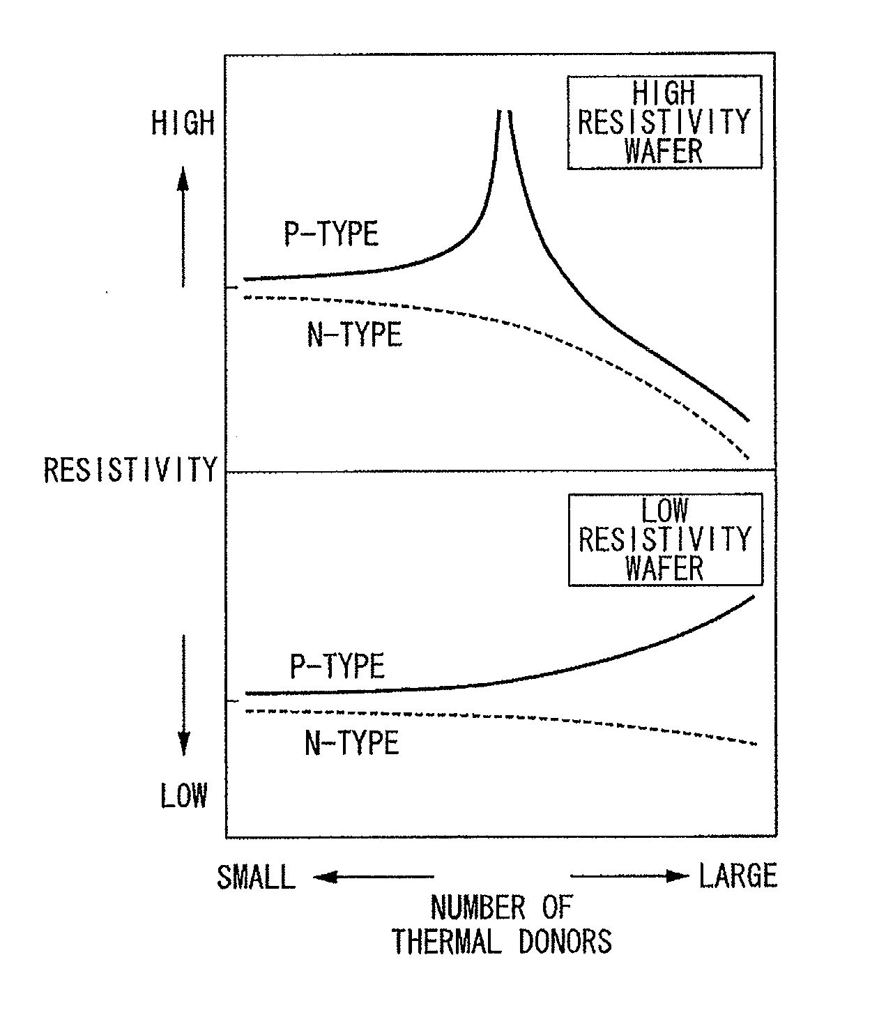
High resistivity silicon wafer and method for manufacturing the same
a technology of high resistivity and silicon wafers, applied in the direction of polycrystalline material growth, chemistry apparatus and processes, crystal growth process, etc., can solve the problems of reducing the productivity of silicon wafers, cmos devices with degraded device characteristics, and wafers with cmos characteristics not reaching desired values or suffering from insufficient n-well separation, etc., to achieve effective prevention of oxygen donors and high resistivity
- Summary
- Abstract
- Description
- Claims
- Application Information
AI Technical Summary
Benefits of technology
Problems solved by technology
Method used
Image

Examples
first embodiment
[0136]A silicon wafer of the present embodiment is a p-type wafer where a denuded zone is formed at or in the vicinity of the surface thereof, and is manufactured by the following production method so as to control a depth range from a surface in which p / n type conversion occurs.
[0137]The production method includes pulling a single crystal such that the single crystal has a dopant concentration at which the wafer surface resistivity becomes in a range of 0.1 to 10 kΩcm, a nitrogen concentration of 1.0×10¹³ to 10×1013 atoms / cm3 (ASTM F-121, 1979) and an oxygen concentration Oi of 5.0×10¹⁷ to 20×1017 atoms / cm3 (ASTM F-121, 1979) by using a Czochralski method, processing the single crystal into wafers by slicing the single crystal, and subjecting the wafer to an oxygen out-diffusion heat treatment process in a non-oxidizing atmosphere.
[0138]Since the silicon wafer is manufactured by the above-described production method, when a heat treatment in a device fabrication process is performe...
second embodiment
[0176]Hereinafter, a silicon wafer according to the present embodiment will be described with reference to the accompanying drawings.
[0177]The silicon wafer of the present embodiment does not include a p / n type conversion region and includes a p-type region with variation in a resistivity distribution set to a range of 0 to 30% across all portions in a wafer thickness direction with respect to a reference value set to a range of 0.1 to 10 kΩcm, and the silicon wafer of the present embodiment is manufactured by a following production method.
[0178]The method includes pulling a single crystal such that the single crystal has a p-type dopant concentration at which a wafer surface resistivity becomes in a range of 0.1 to 10 kΩcm, a nitrogen concentration of 1.0×10¹³ to 10×1013 atoms / cm3 (ASTM F-121, 1979) and an oxygen concentration Oi of 5.0×10¹⁷ to 20×1017 atoms / cm3 (ASTM F-121, 1979) by using a Czochralski method, processing the single crystal into wafers by slicing the single crystal...
third embodiment
[0182]A silicon wafer of the present embodiment is a p-type wafer where a denuded zone is formed at or in the vicinity of the surface thereof, and is manufactured by the following production method so as to control a depth range from a surface in which p / n type conversion occurs.
[0183]The production method includes pulling a single crystal such that the single crystal has a p-type dopant concentration at which a wafer surface resistivity becomes in a range of 0.1 to 10 kΩcm, a carbon concentration of 0.5×10¹⁶ to 10×1016 atoms / cm3 (ASTM F-123, 1981) and an oxygen concentration Oi of 5.0×10¹⁷ to 20×1017 atoms / cm3 (ASTM F-121, 1979) by using a Czochralski method, processing the single crystal into wafers by slicing the single crystal, and subjecting the wafer to an oxygen out-diffusion heat treatment process in a non-oxidizing atmosphere.
[0184]Since the silicon wafer is manufactured by the above-described production method, when a heat treatment in a device fabrication process is perfo...
PUM
| Property | Measurement | Unit |
|---|---|---|
| thickness | aaaaa | aaaaa |
| temperature | aaaaa | aaaaa |
| temperature | aaaaa | aaaaa |
Abstract
Description
Claims
Application Information