

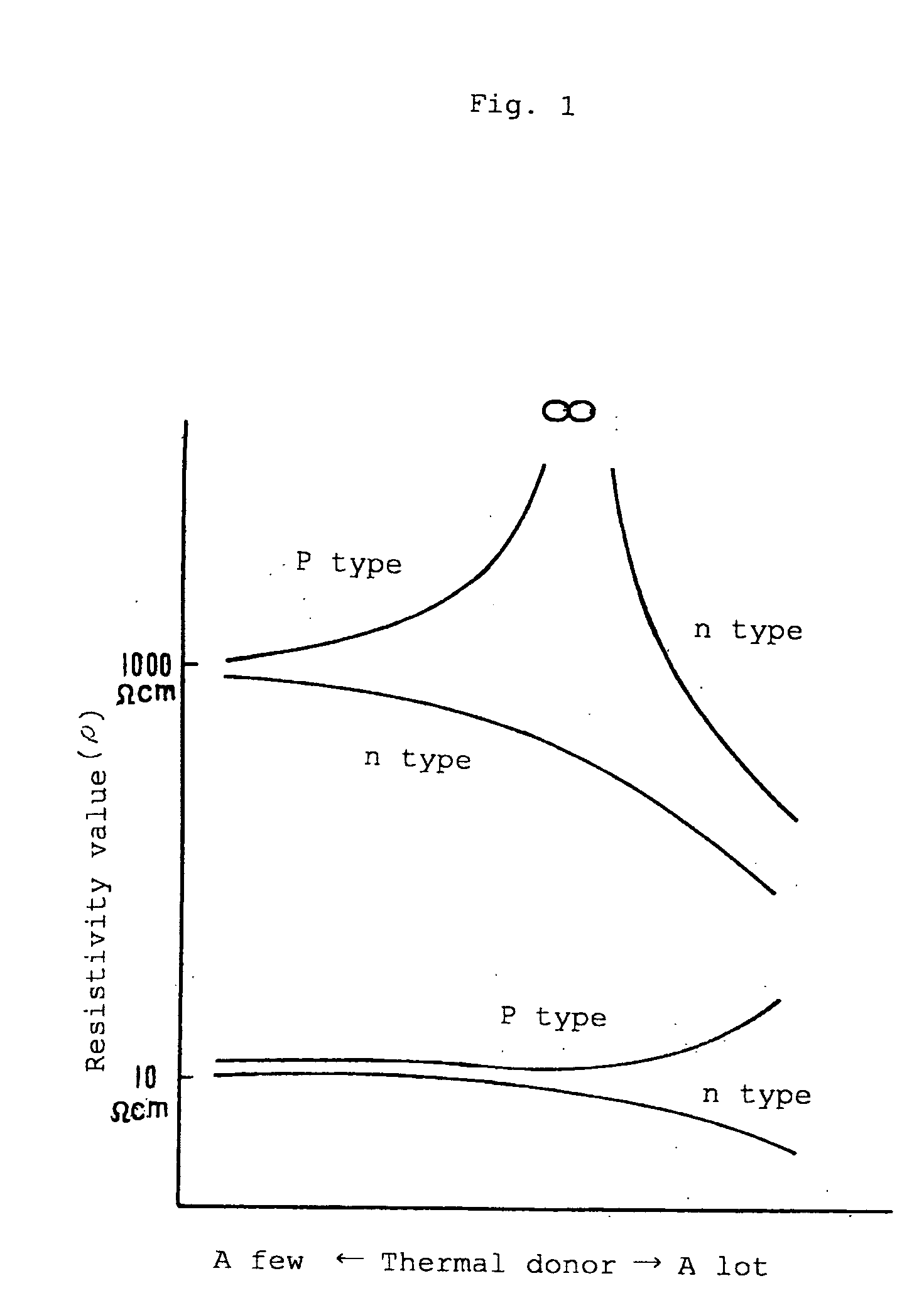
High resistance silicon wafer and method for production thereof
a technology of high resistance and silicon wafer, which is applied in the direction of basic electric elements, electrical equipment, semiconductor devices, etc., can solve the problems of high cost of compound semiconductor substrates, large amount of power required by cmos, and inability to meet the requirements of rf circuits, etc., and achieves uniform gettering ability, and high thermal anneal efficiency.
- Summary
- Abstract
- Description
- Claims
- Application Information
AI Technical Summary
Benefits of technology
Problems solved by technology
Method used
Image

Examples
first embodiment
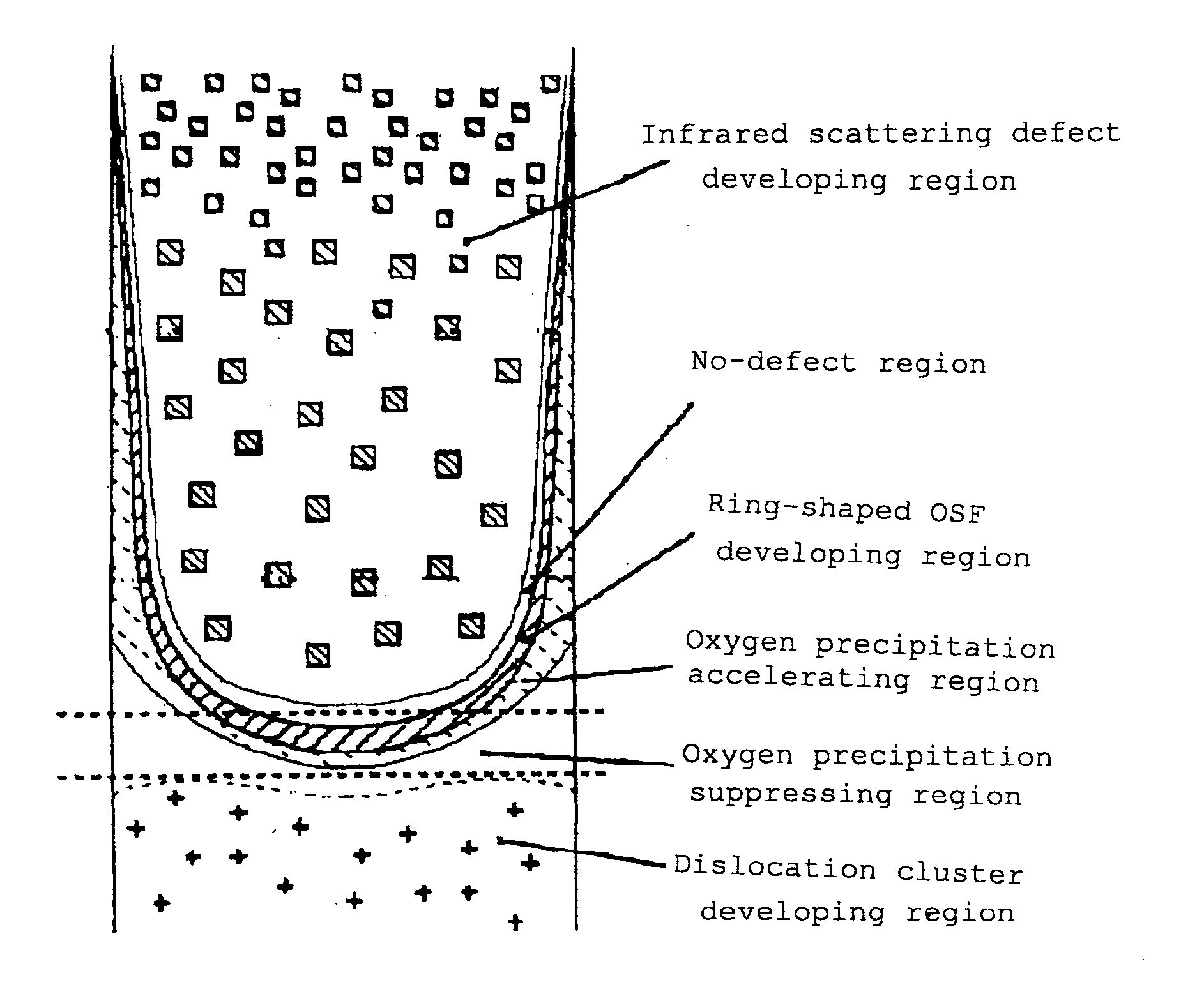
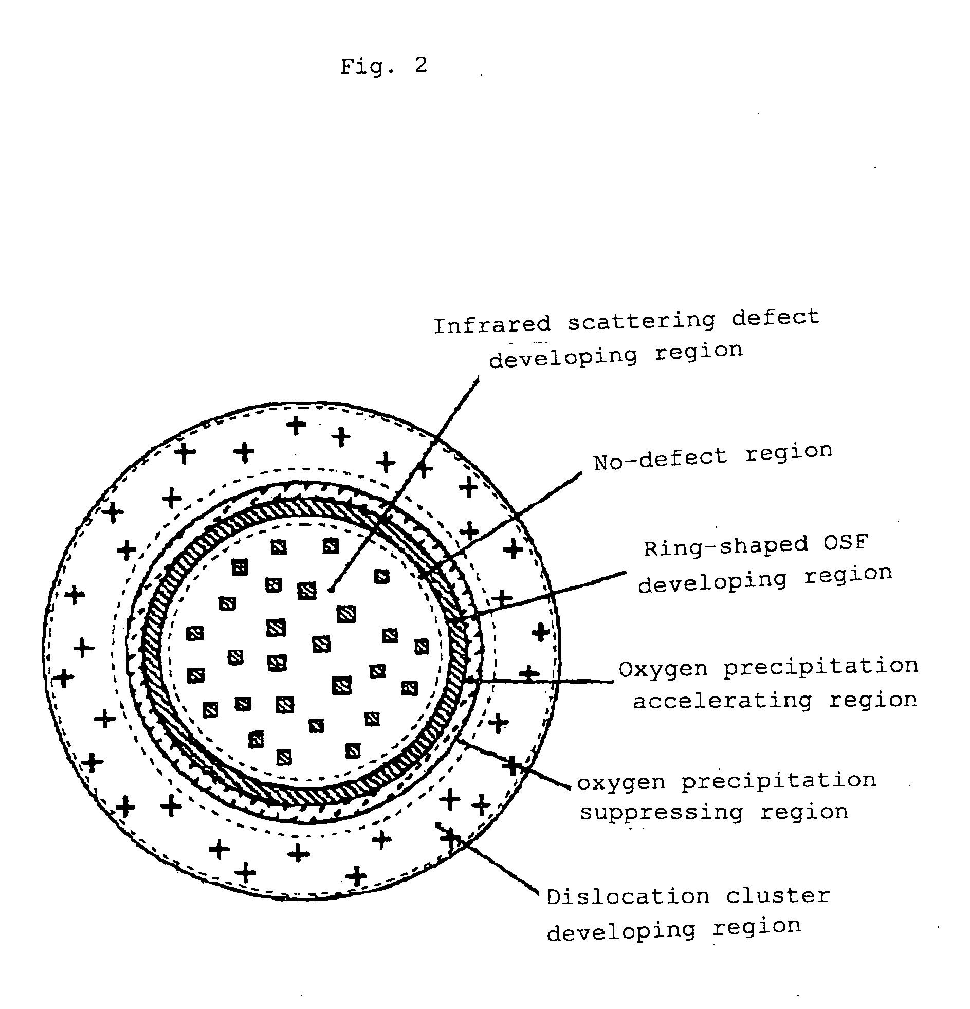
[0050] According to this embodiment, a high-oxygen, high-resistance and carbon-doped silicon single crystal is formed by a normal CZ method and a primary substrate is formed from the silicon single crystal such that an OSF ring exists at a periphery, a COP exists inside, an oxygen concentration is 12×1017 atoms / cm3 (ASTM F-121, 1979) or more, a carbon concentration is 0.5×10¹⁶ atoms / cm3 or more, and resistance is as high as 100 Ω or more at steps S1 to S3.
[0051] If needed, an oxygen outward diffusion heat treatment is performed on the primary substrate at 1100 to 1250° C. for 1 to 5 hours at step S4. By this oxygen outward diffusion heat treatment, an oxygen precipitate (BMD) is prevented from being generated in the heat treatment to be described below. Thus, a DZ (Denuded Zone) layer is formed at least 5 μm in depth from a surface of a product wafer.
[0052] The oxygen outward diffusion heat treatment can be performed in an atmosphere of mixed gas of nitrogen gas and oxygen gas as ...
second embodiment
[0058] According to this embodiment, a crystal free from the COP shown by A-B in FIG. 3 is grown lengthwise in the pulling axis direction by a CZ pulling apparatus in which a hot zone and the like is devised, and a silicon wafer having no defect on the whole surface is provided from the crystal part at steps S1 and S2. More specifically, the wafer having no defect in which a density of the grown-in defect is 1×103 cm−3 or less, which is detected by seco etching. This primary substrate has high oxygen [an oxygen concentration is 14×1017 atoms / cm3 (ASTM F-121, 1979) or more] and high resistance (100 Ωm or more).
[0059] In order to improve the mechanical strength, carbon doping (0.5×10¹⁶ atoms / cm3 or more) can be performed at step S3. In this case, since growth of the oxygen precipitate (BMD) on the wafer surface layer is promoted in the subsequent heat treatment, the oxygen concentration in the primary substrate is allowed to be 12×1017 atoms / cm3 (ASTM F-121, 1979) or more.
[0060] If ...
working example 1
[0098] There were prepared a plurality of 8-inch p-type of sample wafers which were cut out from a normally formed silicon single crystal ingot and on which an oxygen donor eliminating heat treatment was performed at 650° C. for 30 minutes so as to have resistivity of about 750 Ωcm, an oxygen concentration (ASTM F-121, 1979) of about 11×1017 atoms / cm3 and a carbon concentration of about 1×10¹⁶ atoms / cm3. Then, a heat treatment for forming an oxygen precipitate nucleus and a heat treatment for growing the oxygen precipitate were performed like in the comparative example 3 so that a remaining oxygen concentration (ASTM F-121, 1979) might be about 4.5×10¹⁷ atoms / cm3.
[0099] When a density of oxygen precipitate (BMD) having a size of 0.2 μm or more existing in the wafer was measured, it was 4.3 to 6.2×10⁶ / cm2 which was about the same as that in the comparative example 4, in which the remaining oxygen concentration (ASTM F-121, 1979) was lowered from the initial oxygen concentration (AST...
PUM
 Abstract
Description
Claims
Application Information