Composite gate structure in an integrated circuit

a gate structure and integrated circuit technology, applied in the field of semiconductor devices, can solve the problems that the integrated circuit and manufacturing process, however, cannot meet all requirements of the integrated circuit, and one mos design cannot meet all requirements, so as to improve the performance of the integrated circuit and reduce the step height between the gate stacks of different devices.

Active Publication Date: 2007-02-27
TAIWAN SEMICON MFG CO LTD
View PDF26 Cites 59 Cited by
  • Summary
  • Abstract
  • Description
  • Claims
  • Application Information

AI Technical Summary

Benefits of technology

[0010]In accordance with yet another aspect of the present invention, the first MOS device is an nMOS device, and the first metal gate has a work function of less than about 4.6 eV. The second MOS device is a pMOS device, and the second metal gate has a work function of greater than about 4.8 eV. The balanced work functions improve the performance of the integrated circuit.
[0011]In accordance with yet another aspect of the present invention, each of the gate stacks of the first and second MOS devices further includes a silicon portion over the respective first metal gate and second metal gate. The step heights between the gate stacks of different devices are reduced by adding the silicon portion. Preferably, the gate stack of the second device further includes an additional metal gate over the first metal gate, and the additional metal gate is simultaneously formed as the second metal gate of the second MOS device is formed.

Problems solved by technology

Technology advancement demands more and more functions to be integrated on a single chip, and thus one MOS design cannot fulfill all requirements in an integrated circuit.
Scaling of the integrated circuit also causes other problems.
However, polysilicon has depletion problems, so metal gate electrodes were introduced, particularly for device formation in core regions, to avoid the poly depletion phenomenon.
Previously discussed issues demand customized manufacturing processes.
These integrated circuits and manufacturing processes, however, have a potential problem.
This step height adds complexity and cost for subsequent manufacturing processes.

Method used


Image

  • Composite gate structure in an integrated circuit
  • Composite gate structure in an integrated circuit
  • Composite gate structure in an integrated circuit

Examples


Embodiment Construction

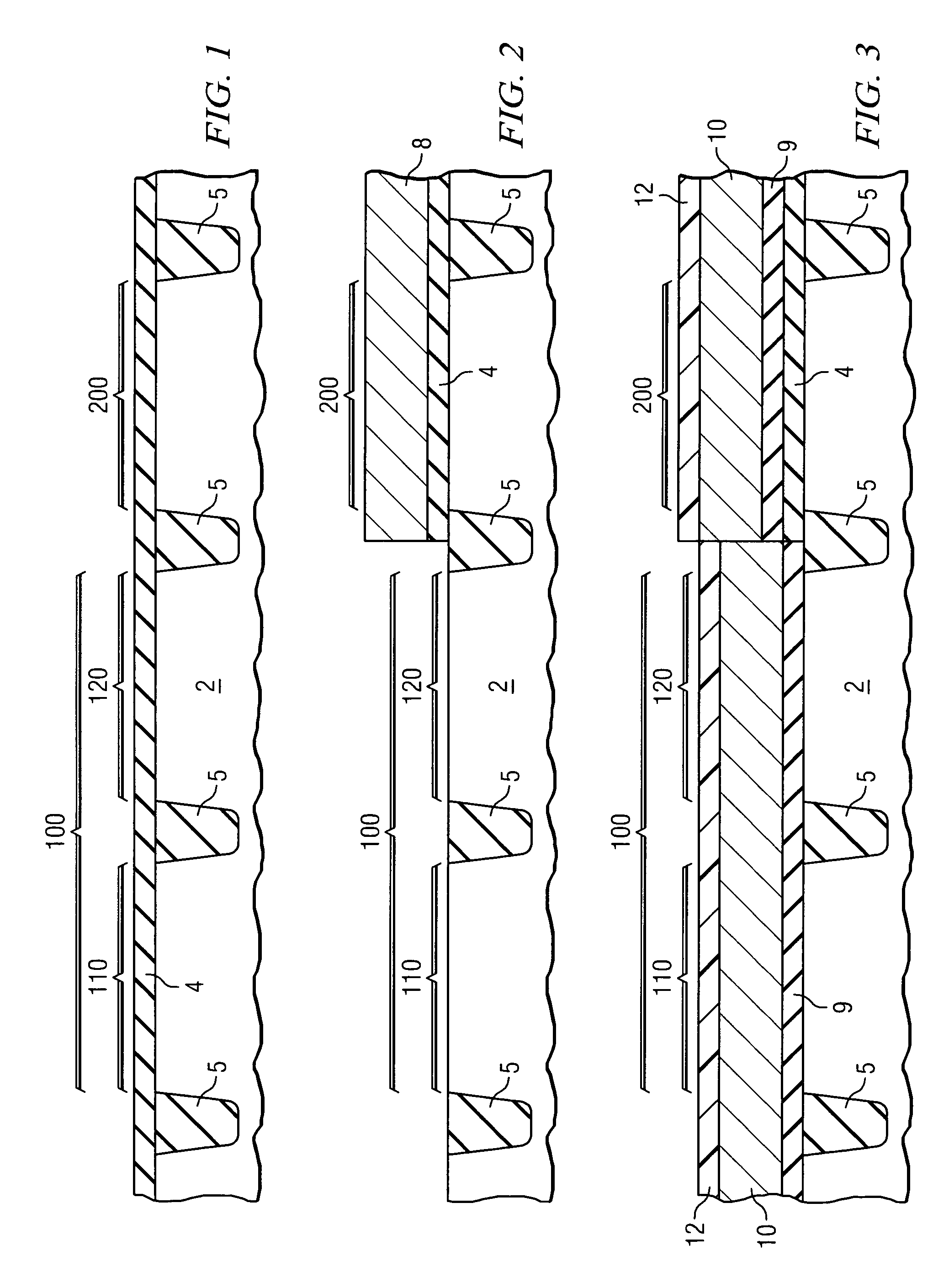
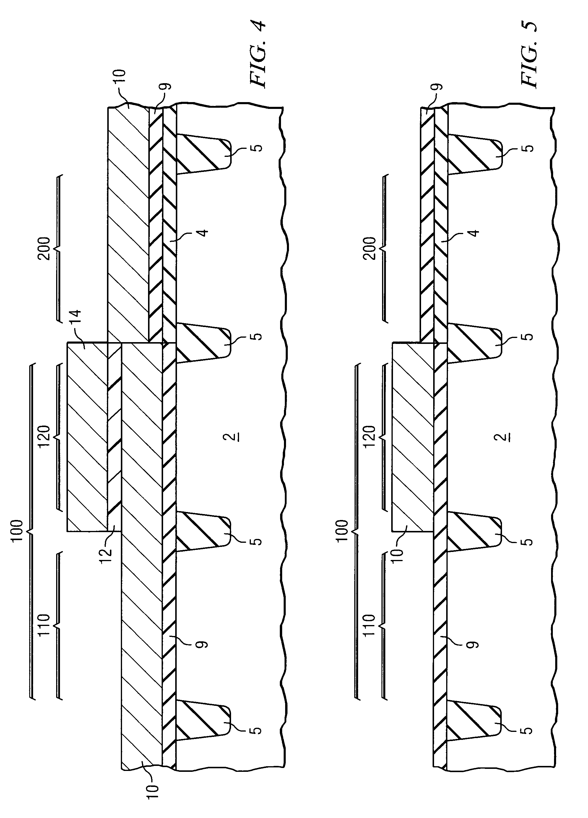
[0014]The making and using of the presently preferred embodiments are discussed in detail below. It should be appreciated, however, that the present invention provides many applicable inventive concepts that can be embodied in a wide variety of specific contexts. The specific embodiments discussed are merely illustrative of specific ways to make and use the invention, and do not limit the scope of the invention.

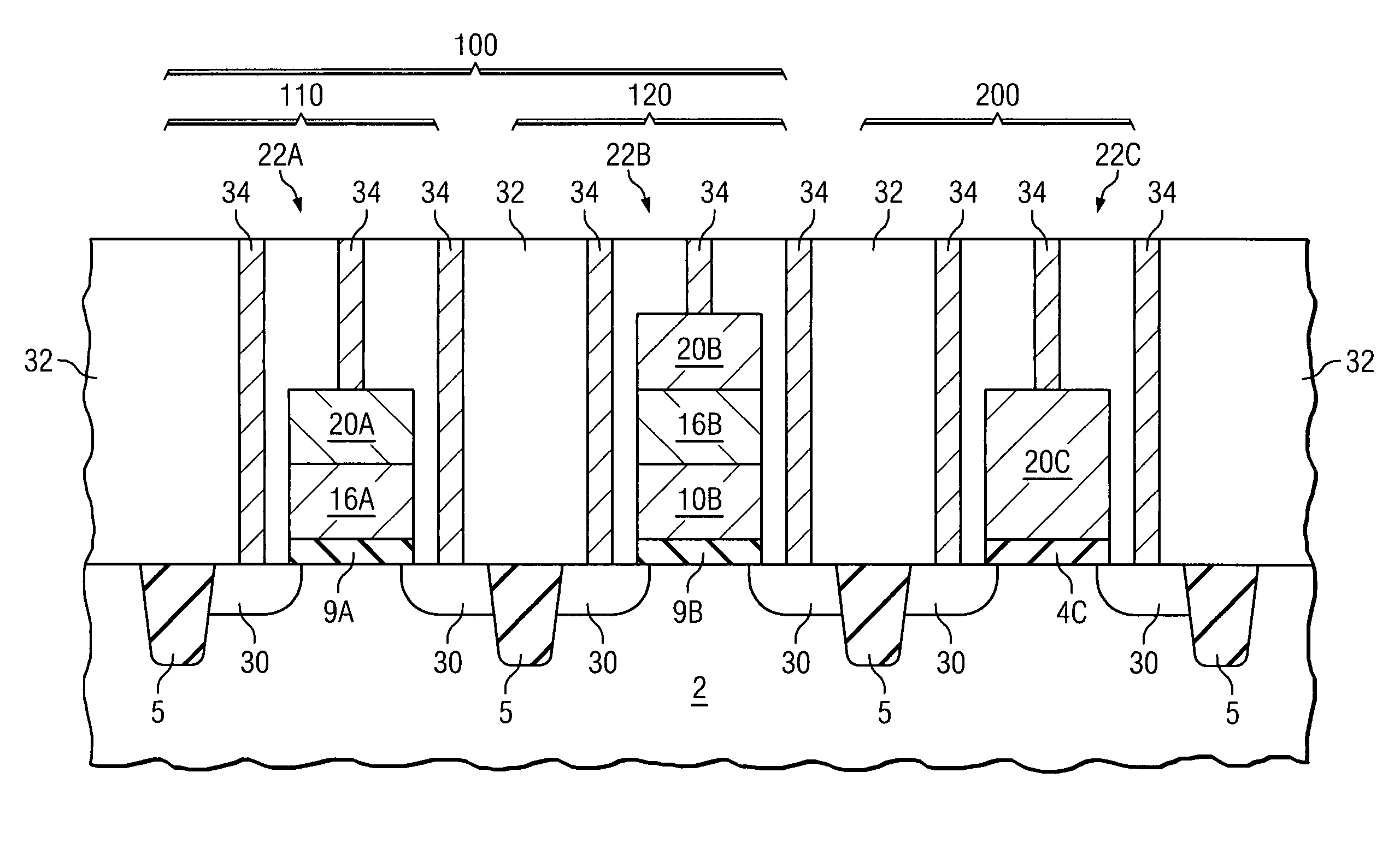
[0015]In the preferred embodiments of the present invention, a chip includes two regions, a first region and a second region. The devices in the first region and the second region have different designs and thus are customized for different functions. For example, the first region may be a core region wherein high performance is required, and the second region may be a peripheral region such as an I / O region, an analog region, a high voltage device region, or a region for devices such as polysilicon resistors, decoupling capacitors, etc.

[0016]The preferred embodiments are ill...


PUM


Abstract

An integrated circuit having composite gate structures and a method of forming the same are provided. The integrated circuit includes a first MOS device, a second MOS device and a third MOS device. The gate stack of the first MOS device includes a high-k gate dielectric and a first metal gate on the high-k gate dielectric. The gate stack of the second MOS device includes a second metal gate on a high-k gate dielectric. The first metal gate and the second metal gate have different work functions. The gate stack of the third MOS device includes a silicon gate over a gate dielectric. The silicon gate is preferably formed over the gate stacks of the first MOS device and the second MOS device.

Description

CROSS-REFERENCE TO RELATED APPLICATIONS[0001]This application relates to the following co-pending and commonly assigned patent application: U.S. patent application Ser. No. 10 / 832,020, filed Apr. 26, 2004, entitled “Semiconductor Device with High-K Gate Dielectric”, which application is incorporated herein by reference.TECHNICAL FIELD[0002]This invention relates generally to semiconductor devices, and more specifically to the gate formation of MOS devices.BACKGROUND[0003]CMOS has been the basic logic building block in the digital-dominant world for decades. Device dimensions have been continuously shrunk in order to achieve higher performance as well as higher packing density. Technology advancement demands more and more functions to be integrated on a single chip, and thus one MOS design cannot fulfill all requirements in an integrated circuit. For example, in a traditional circuit that employs micron technology or earlier technologies, the operation voltage of the core circuit was...

Claims


Application Information

Patent Timeline
Patent Type & Authority Patents(United States)
IPC IPC(8): H01L29/76
CPCH01L21/823842H01L21/823857H01L29/785
Inventor WU, I-LUCHEN, KUANG-HSINHAN, LIANG-KAI
Owner TAIWAN SEMICON MFG CO LTD
Why Eureka
Try Eureka