Bipolar transistor with lattice matched base layer

a bipolar transistor and base layer technology, applied in the direction of basic electric elements, electrical apparatus, semiconductor devices, etc., can solve the problems of conduction band spike at the emitter-base interface, limit the usefulness of devices for low power applications, etc., to reduce the injection of reverse holes, and improve the management of voltage budgets

Inactive Publication Date: 2007-03-06
IQE KC
View PDF21 Cites 82 Cited by
  • Summary
  • Abstract
  • Description
  • Claims
  • Application Information

AI Technical Summary

Benefits of technology

[0006]The present invention provides an HBT having an n-doped collector, a base formed over the collector and composed of a III-V material that includes indium and nitrogen, and an n-doped emitter formed over the base. The III-V material of the base layer has a carbon dopant concentration of about 1.5×1019 cm−3 to about 7.0×1019 cm−3. In a preferred embodiment, the base layer includes the elements gallium, indium, arsenic, and nitrogen. The presence of nitrogen in the material and the high dopant concentration of the materials of the invention reduce the band gap and the sheet resistivity (Rsb) of the material which results in a lower turn-on voltage. The HBTs of the present invention have a lower turn-on voltage than GaAs-based HBTs of the prior art.
[0007]In a preferred embodiment, the III-V compound material system can be represented by the formula Ga1-xInxAs1-yNy. It is known that the energy-gap of Ga1-xInxAs drops substantially when a small amount of nitrogen is incorporated into the material. Moreover, because nitrogen pushes the lattice constant in the opposite direction from indium, Ga1-xInxAs1-yNy, alloys can be grown lattice-matched to GaAs by adding the appropriate ratio of indium to nitrogen to the material. Thus, excess strain which results in an increased band gap and misfit dislocation of the material can be eliminated. The ratio of indium to nitrogen is thus selected to reduce or eliminate strain. In a preferred embodiment of the present invention, x=3y in the Ga1-xInxAs1-yNy base layer of the HBT.
[0011]Another method of minimizing the conduction band spike is to include one or more transitional layers between the heterojunction. Transitional layers having low band gap set back layers, graded band gap layers, doping spikes or a combination thereof can be used to minimize the conduction band spike. In addition, one or more lattice-matched layers can be present between the base and emitter or base and collector to reduce the lattice strain on the materials at the heterojunction.
[0012]The present invention also provides a method of fabricating an HBT and a DHBT. The method involves growing a base layer composed of gallium, indium, arsenic and nitrogen over an n-doped GaAs collector. The base layer is grown using an internal and external carbon source to provide carbon doped base layer. An n-doped emitter layer is then grown over the base layer. The use of an internal and external carbon source to provide the carbon dopant for the base layer results in a material with a higher carbon dopant concentration than has been achieved in the prior art. Typically, dopant levels of about 1.5×1019 cm−3 to about 7.0×1019 cm−3 are achieved using the method of the invention. In a preferred embodiment, dopant levels of about 3.0×1019 cm−3 to about 7.0×1019 cm−3 are achieved with the method of the invention. A higher dopant concentration in a material reduces the sheet resistivity and band gap of the material. Thus, the higher the dopant concentration in the base layer of an HBT and DHBT, the lower the turn on voltage of the device.
[0014]The reduction in turn-on voltage allows for better management of the voltage budget on both wired and wireless GaAs-based RF circuits, which are constrained either by standard fixed voltage supplies or by battery output. Lowering the turn-on voltage also alters the relative magnitude of the various base current components in a GaAs-based HBT. DC current gain stability as a function of both junction temperature and applied stress has been previously shown to rely critically on the relative magnitudes of the base current components. The reduction in reverse hole injection enabled by a low turn-on voltage is favorable for both the temperature stability and long-term reliability of the device. Thus, strain free Ga1-xInxAs1-yNy base materials having a high dopant concentration enhance RF performance in GaAs-based HBTs and DHBTs.

Problems solved by technology

The turn-on voltage can limit the usefulness of devices for low power applications in which supply voltages are constrained by battery technology and the power requirements of other components.
HBTs, however, can suffer from the disadvantage of having an abrupt discontinuity in the band alignment of the semiconductor material at the heterojunction can lead to a conduction band spike at the emitter-base interface of the HBT.

Method used


Image

  • Bipolar transistor with lattice matched base layer
  • Bipolar transistor with lattice matched base layer
  • Bipolar transistor with lattice matched base layer

Examples


Embodiment Construction

[0022]The foregoing and other objects, features and advantages of the invention will be apparent from the following more particular description of preferred embodiments of the invention, as illustrated in the accompanying drawings in which like reference characters refer to the same parts throughout the different views. The drawings are not necessarily to scale, emphasis instead being placed upon illustrating the principles of the invention.

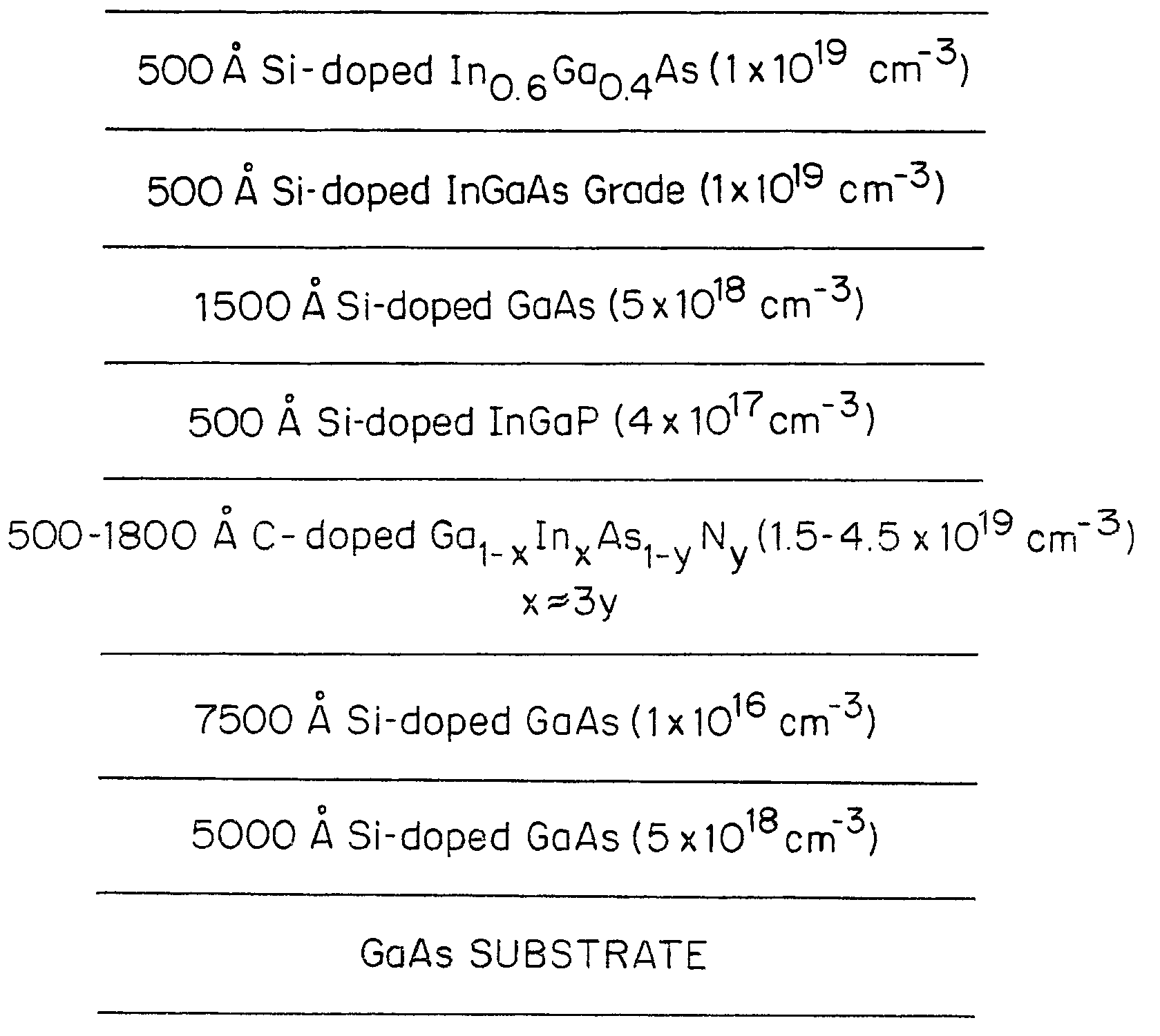
[0023]A III-V material is a semiconductor having a lattice comprising at least one element from column III(A) of the periodic table and at least one element from column V(A) of the periodic table. In one embodiment, the III-V material is a lattice comprised of gallium, indium, arsenic and nitrogen. Preferably, the III-V material can be represented by the formula Ga1-xInxAs1-yNy wherein x and y are each, independently, about 1.0×10⁻⁴ to about 2.0×10⁻¹. More perferably, x is about equal to 3y. In a most preferred embodiment, x and 3y are about 0.01...


PUM

PropertyMeasurementUnit
temperatureaaaaaaaaaa
band gapaaaaaaaaaa

Abstract

A semiconductor material which has a high carbon dopant concentration and is composed of gallium, indium, arsenic and nitrogen is disclosed. The material is useful in forming the base layer of gallium arsenide based heterojunction bipolar transistors because it can be lattice matched to gallium arsenide by controlling the concentration of indium and nitrogen. The disclosed semiconductor materials have a low sheet resistivity because of the high carbon dopant concentration obtained.

Description

RELATED APPLICATION[0001]This application is a divisional of U.S. application Ser. No. 09 / 995,079, filed on Nov. 27, 2001 (now U.S. Pat. No. 6,750,480 B2), which claims the benefit of U.S. Provisional Application No. 60 / 253,159, filed on Nov. 27, 2000, the teachings of both of which are incorporated herein in their entirety.GOVERNMENT SUPPORT[0002]The invention was supported, in whole or in part, by grant F33615-99-C-1510 from the Small Business Technology Transfer (STTR) Program of the U.S. Air Force. The government has certain rights in the invention.BACKGROUND OF THE INVENTION[0003]Bipolar junction transistors (BJT) and heterojunction bipolar transistor (HBT) integrated circuits (ICs) have developed into an important technology for a variety of applications, particularly as power amplifiers for wireless handsets, microwave instrumentation, and high speed (>10 Gbit / s) circuits for fiber optic communication systems. Future needs are expected to require devices with lower voltage...

Claims


Application Information

Patent Timeline
Patent Type & Authority Patents(United States)
IPC IPC(8): H01L21/331H01L29/10H01L29/20H01L29/737
CPCH01L29/1004H01L29/7371H01L29/66318H01L29/2003
Inventor WELSER, ROGER E.DELUCA, PAUL M.PAN, NOREN
Owner IQE KC
Why Eureka
Try Eureka