
Reducing memory failures in integrated circuits

a technology of integrated circuits and memory failures, applied in the field of reducing memory failures in integrated circuits, can solve problems such as system failure, error, and erroneous 1 bit of data words, and achieve the effects of improving reliability, improving reliability, and improving memory reliability

Inactive Publication Date: 2007-03-06
POLARIS INNOVATIONS
View PDF10 Cites 17 Cited by
  • Summary
  • Abstract
  • Description
  • Claims
  • Application Information

AI Technical Summary

Benefits of technology

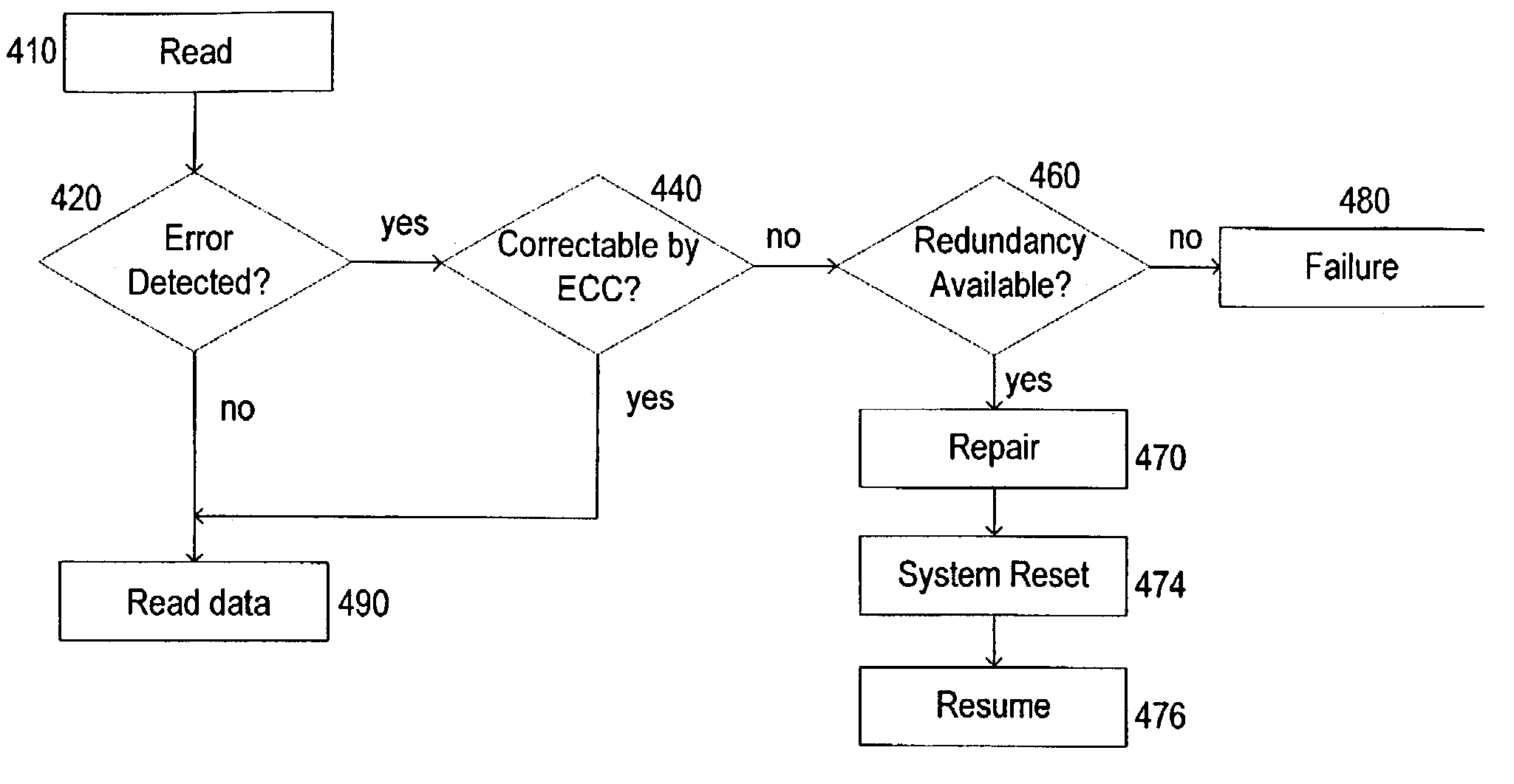
[0006]The invention relates to improving reliability of memory. More particularly, the invention relates to improving reliability using error correction and redundancy. In one embodiment, a method of improving memory reliability comprises retrieving a data word from memory. Error correction code is used to determine if the data word contains any errors or not. If the data word contains an error, memory redundancy is used to repair at least the memory cell corresponding to the error. In one embodiment, redundancy is used if the data word contains an error which cannot be corrected by error correction code.

Problems solved by technology

When a data word is accessed, errors may occur.
For example, 1 bit of the data word can be erroneous due to a defective memory cell.
However, in the event that the number of errors in a data word exceed the capabilities of a particular ECC, a system failure would occur.
For example, for ECC capable of repairing one bit, a second failing bit within the accessed data word would lead to a total failure.

Method used


Image

  • Reducing memory failures in integrated circuits
  • Reducing memory failures in integrated circuits
  • Reducing memory failures in integrated circuits

Examples


Embodiment Construction

[0011]The invention relates to reducing memory failures. The invention can be applicable to, for example, various types of processing systems. A system can include, for example, a processor which accesses one or more memory ICs. Alternatively, the processor and the memory array can be integrated into a single IC, such as a system on a chip (SOC). one embodiment, the memory array can include volatile or non-volatile memory cells.

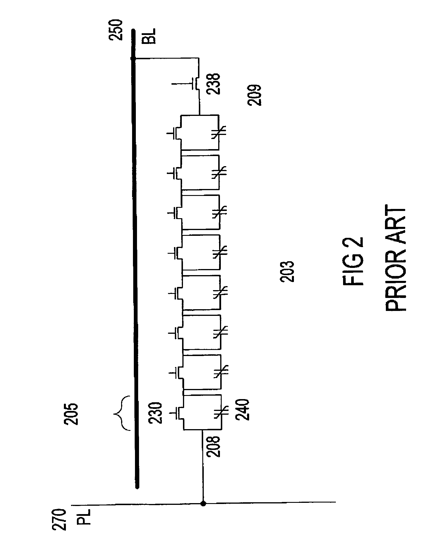
[0012]In one embodiment, the memory array comprises non-volatile memory cells. Other types of memory cells are also useful. Preferably, the nonvolatile memory cells are ferroelectric memory cells, such as those described in FIG. 1. The memory cells can be arranged in a folded or open bitline architecture. Other types of memory architectures, such as series architectures, are also useful. Series architectures are described in, for example, US patent titled “Semiconductor Memory Device and Various Systems Mounting Them”, U.S. Pat. No. 5,903,492, filed on Jun. 1...


PUM


Abstract

Memory reliability is improved by using redundancy to repair errors detected by ECC. In one embodiment, redundancy repairs errors which cannot be corrected by ECC. The redundancy can employ the use of electronic fuses, enabling repairs after an IC containing the memory is packaged. Redundancy can also be performed prior to packaging of the IC.

Description

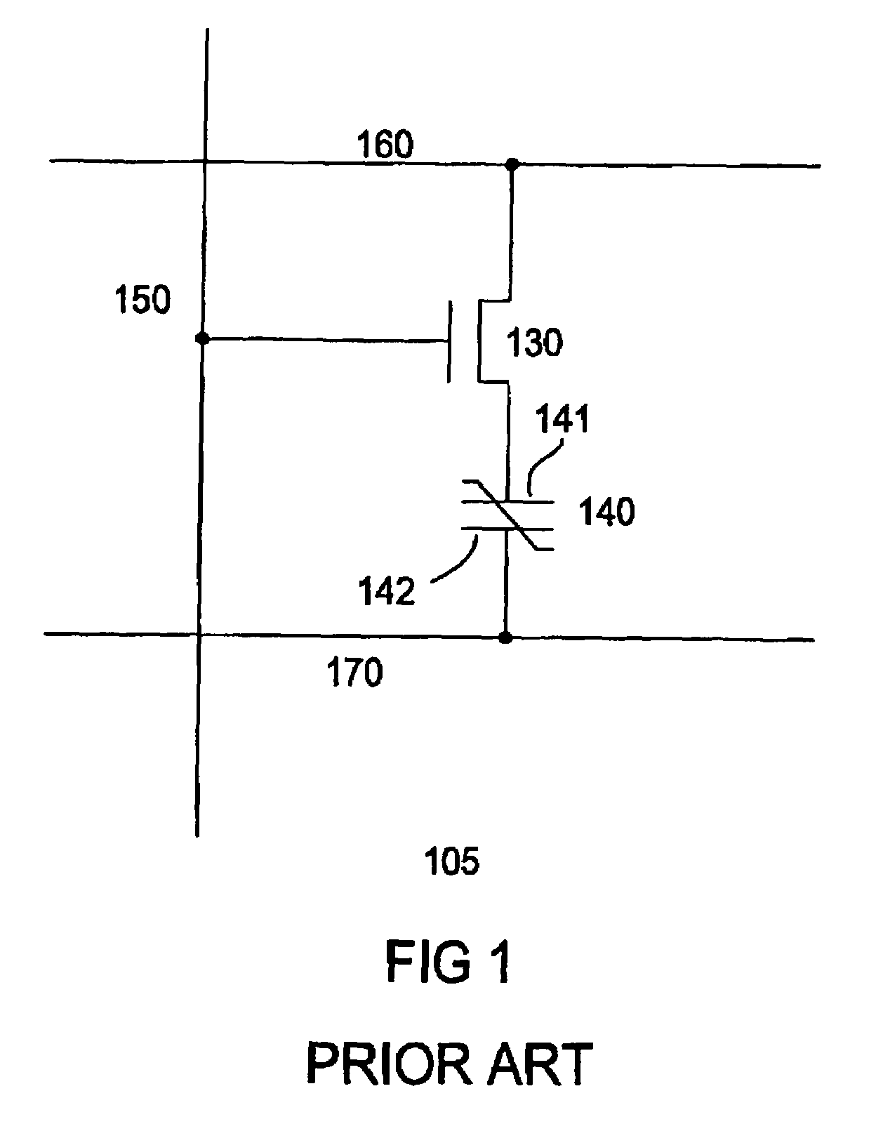
BACKGROUND OF INVENTION[0001]Non-volatile memory cells, such as ferroelectric memory cells, are used in semiconductor memory devices. Such ferroelectric memory cells employ the use of ferroelectric metal oxide ceramic materials, such as lead zirconate titanate (PZT). Other types of ferroelectric material, such as Strontium-bismuth-tantalate (SBT) or lead-lanthanum-zirconium-titanate (PLZT) may also be used. FIG. 1 shows a ferroelectric memory cell 105 having a transistor 130 and a ferroelectric capacitor 140. A capacitor electrode 142 is coupled to a plateline 170 and another capacitor electrode 141 is coupled to the transistor which selectively couples or decouples the capacitor from a bitline 160, depending on the state (active or inactive) of a wordline 150 coupled to the transistor gate. A plurality of memory cells are interconnected by wordlines, bitlines, and plateline(s). Support circuitry is provided to facilitate access to the memory cells.[0002]The ferroelectric memory sto...

Claims


Application Information

Patent Timeline
Patent Type & Authority Patents(United States)
IPC IPC(8): G11C29/42G11C11/22G11C29/04G11C29/24G06F11/10G11C29/00
CPCG06F11/1008G11C29/72G11C11/22
Inventor WOHLFAHRT, JOERGROEHR, THOMASJACOB, MICHAEL
Owner POLARIS INNOVATIONS
Learn More