Active matrix type liquid crystal display apparatus
- Summary
- Abstract
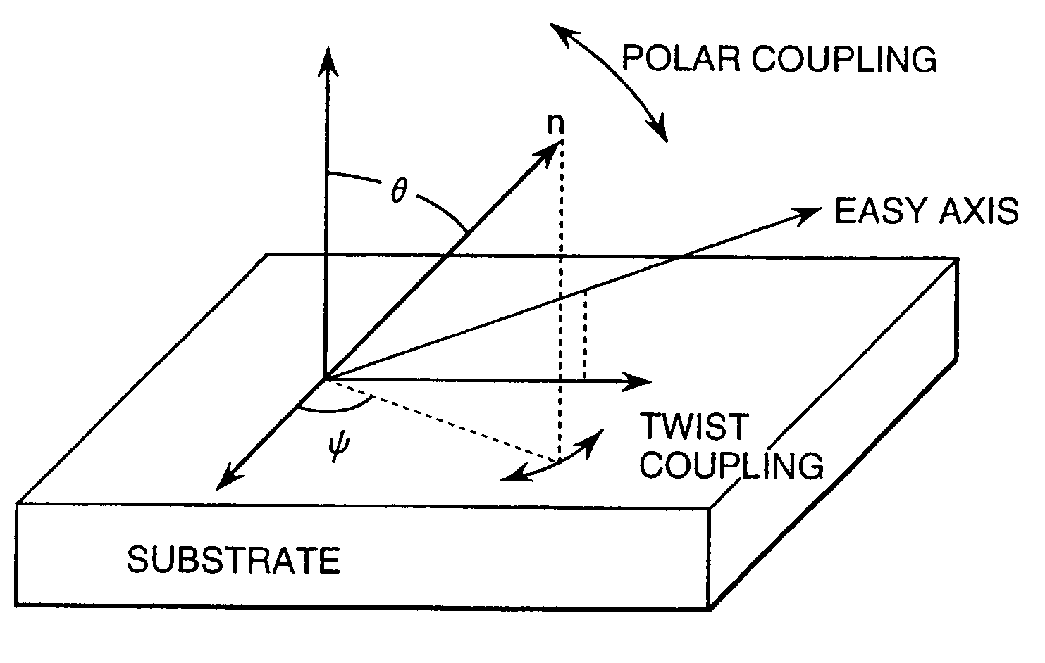
- Description
- Claims
- Application Information
AI Technical Summary
Benefits of technology
Problems solved by technology
Method used
Image

Examples
embodiment 1
[Embodiment 1]
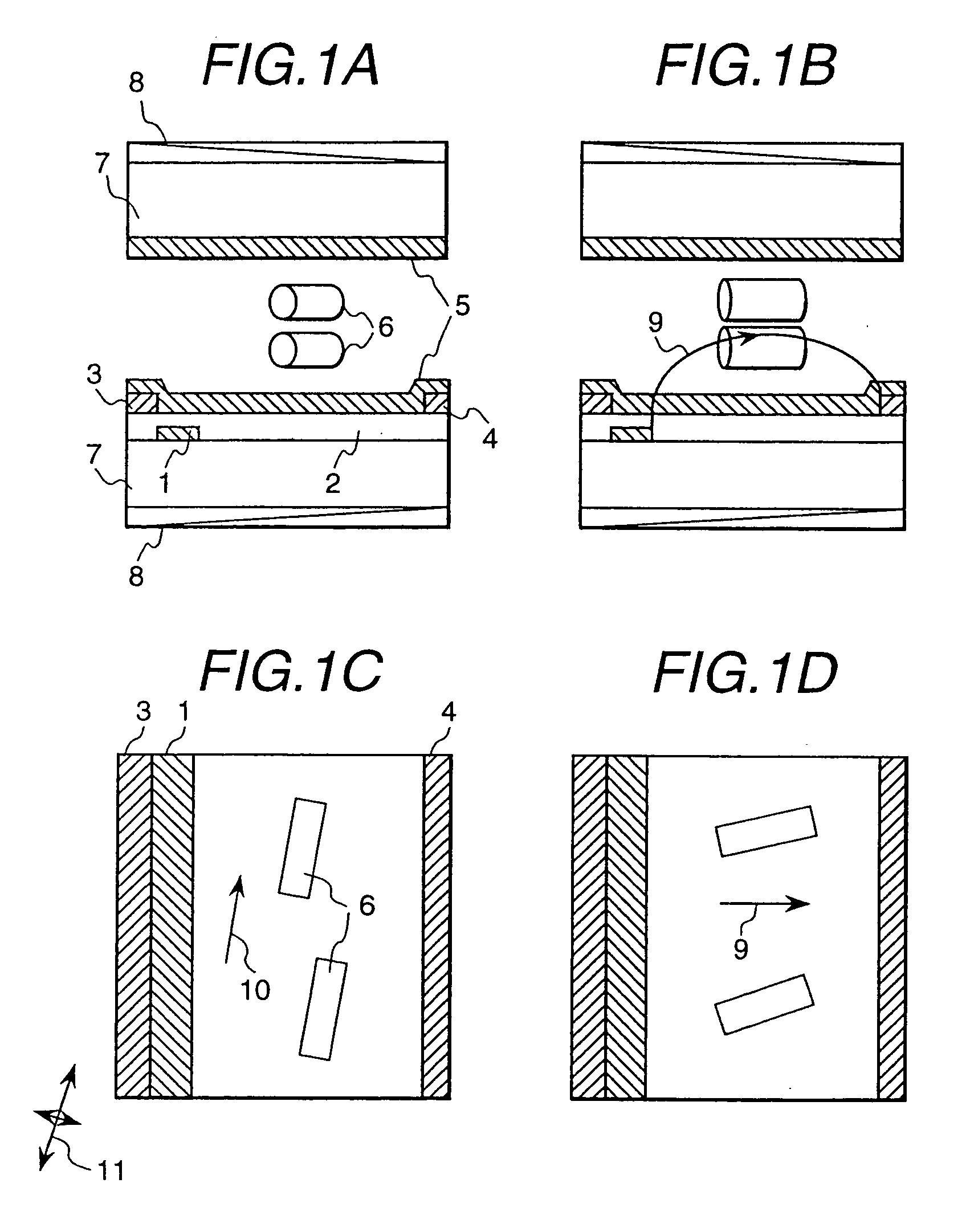
[0049]Using two surface-finished transparent glass substrates having a thickness of 1.1 mm as substrates, thin film transistors and wiring electrodes capable of applying an in-plane electric field were formed on one of the substrates, and an insulator preventive film made of silicon nitride was further formed on the uppermost surface. The structure of the thin film transistor and the various kinds of electrodes is shown in FIG. 4 in a front view as seen from a direction perpendicular to the substrate surface, and in the cross-sectional side views of FIGS. 4A and 4B, which are taken on the planes of the lines A–A′ and B–B′ of the front view.
[0050]The thin film transistor element 14 is composed of pixel electrodes (source electrodes) 4, a signal electrode (drain electrode) 3, a scanning electrode (gate electrode) 12 and amorphous silicon 13. Common electrodes 1 and the scanning electrode 12, and the signal electrode 3 and the pixel electrode 4 are respectively formed by ...
embodiment 2
[Embodiment 2]
[0063]This embodiment is similar to Embodiment 1 except for the alignment layer which is used. Polyamic acid varnish was obtained by dissolving m-phenylene-diamine of 1.0 mole % in N-methyl-2-pyrrolidone, and adding 3,3′,4,4′-diphenyl-ether carboxylic acid anhydride of 1 mole % to the solution to react for 6 hours at 40° C. The polyamic acid varnish had a weight average molecular weight of approximately 21,000 in a standard styrene base, and a weight average molecular weight / number average molecular weight (MW / MN) of approximately 1.8. A closely packed polyimide alignment layer of approximately 600 Å was formed by diluting the varnish to 6% concentration, adding γ-aminopropyl-triethoxy-silane of 0.3 weight % in a sold base, and then printing and performing heat treatment of 225° C. / 30 minutes.
[0064]The surface modulus of elasticity of a polyimide alignment layer obtained through the same fabrication method as described above was evaluated using a scanning viscoelastici...
embodiment 3
[Embodiment 3]
[0069]This embodiment is similar to Embodiment 1 except for the alignment layer being used. Polyamic acid varnish was prepared by dissolving 4,4′-diamino-diphenyl methane of 1.0 mole % in a mixed solvent of N-methyl-2-pyrrolidone and dimethylacetamide, and adding 1,2,3,4-cyclopenthane carboxylic acid anhydride of 1 mole % to the solution to react for 12 hours at 30° C. The polyamic acid varnish had a weight average molecular weight of approximately 12,000 to 250,000 in a standard styrene base. After that, using gel permeation chromatography, the varnish was classified and collected to obtain a single disperse polyamic acid varnish having a weight average molecular weight of approximately 150,000, and a weight average molecular weight / number average molecular weight (MW / MN) of approximately 1.51. A closely packed polyimide alignment layer of approximately 600 Å was formed by diluting the varnish to 6% concentration, adding γ-aminopropyl-triethoxy-silane of 0.3 weight % ...
PUM
| Property | Measurement | Unit |
|---|---|---|
| Length | aaaaa | aaaaa |
| Angle | aaaaa | aaaaa |
| Electric charge | aaaaa | aaaaa |
Abstract
Description
Claims
Application Information