

Method and apparatus for optimization of digital integrated circuits using detection of bottlenecks
- Summary
- Abstract
- Description
- Claims
- Application Information
AI Technical Summary
Benefits of technology
Problems solved by technology
Method used
Image

Examples
Embodiment Construction
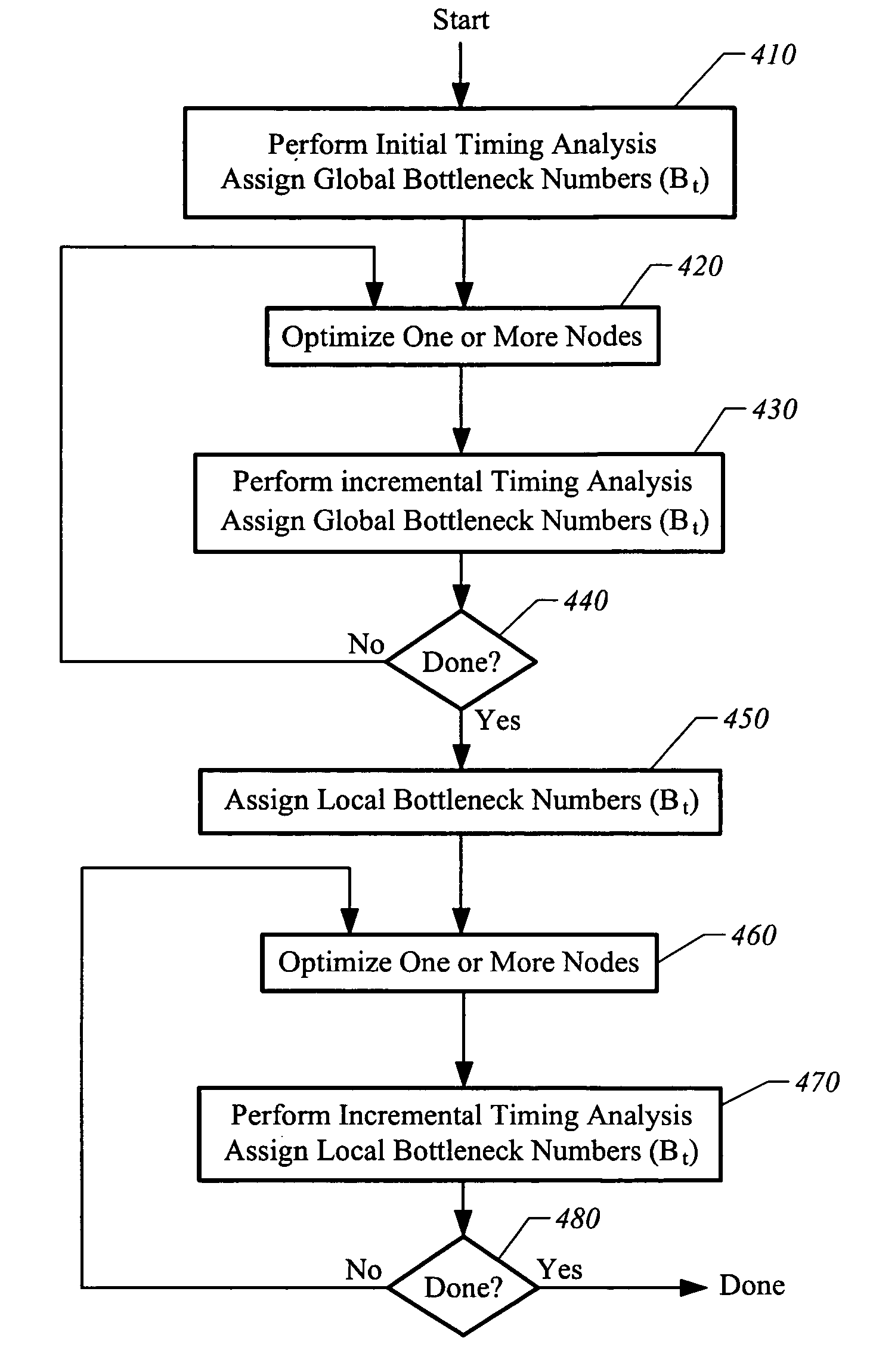
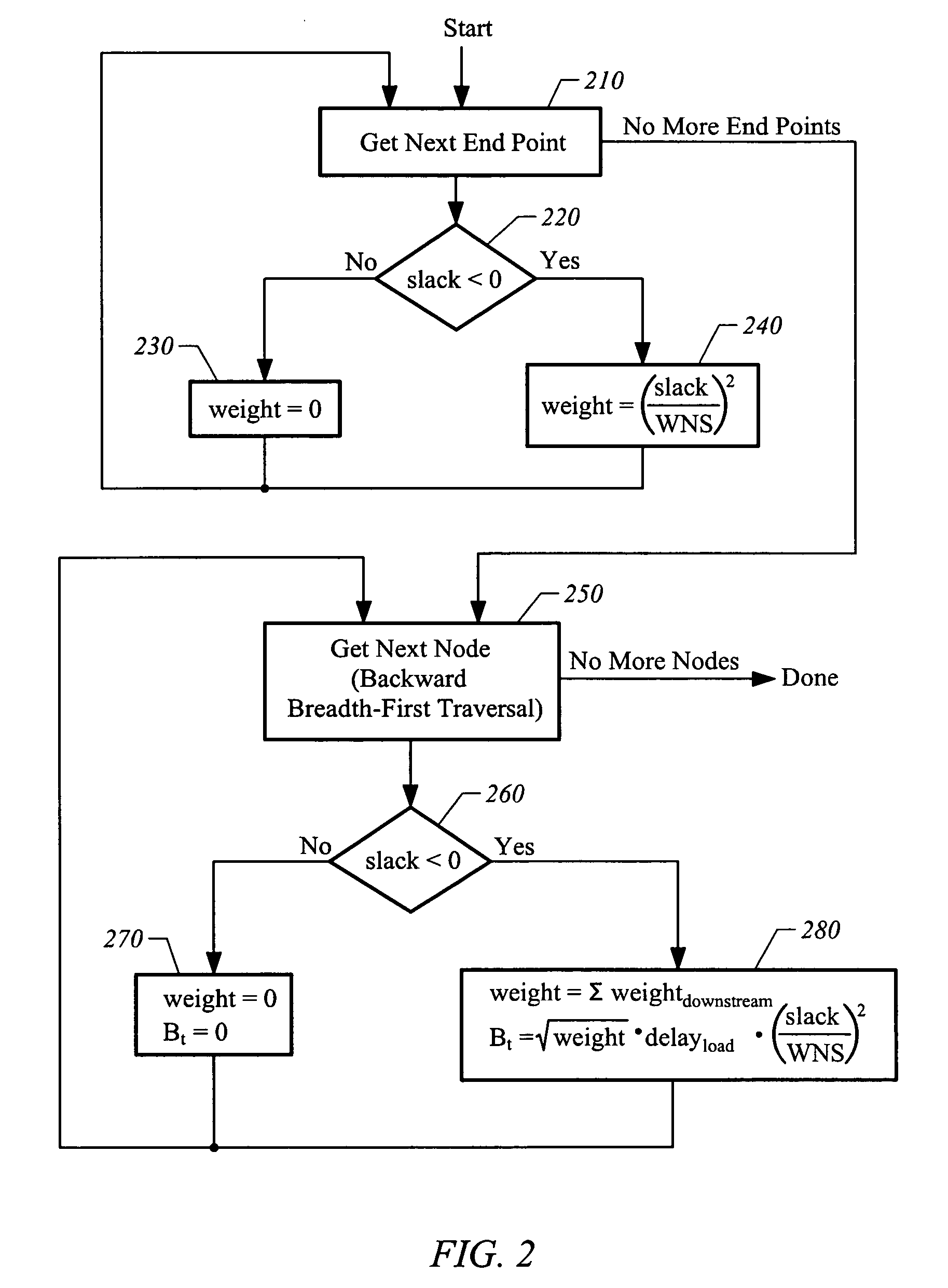
[0021]The present invention dramatically reduces the computational effort to perform physical synthesis on large circuit graphs by using a new technique that identifies “bottleneck” nodes in the circuit graph and optimizes these bottleneck nodes. This approach performs a global analysis of the design for performance bottlenecks and dramatically reduces the execution time of physical synthesis in that no path enumeration is required. The approach is computationally very efficient and also robust in the presence of bad constraints.
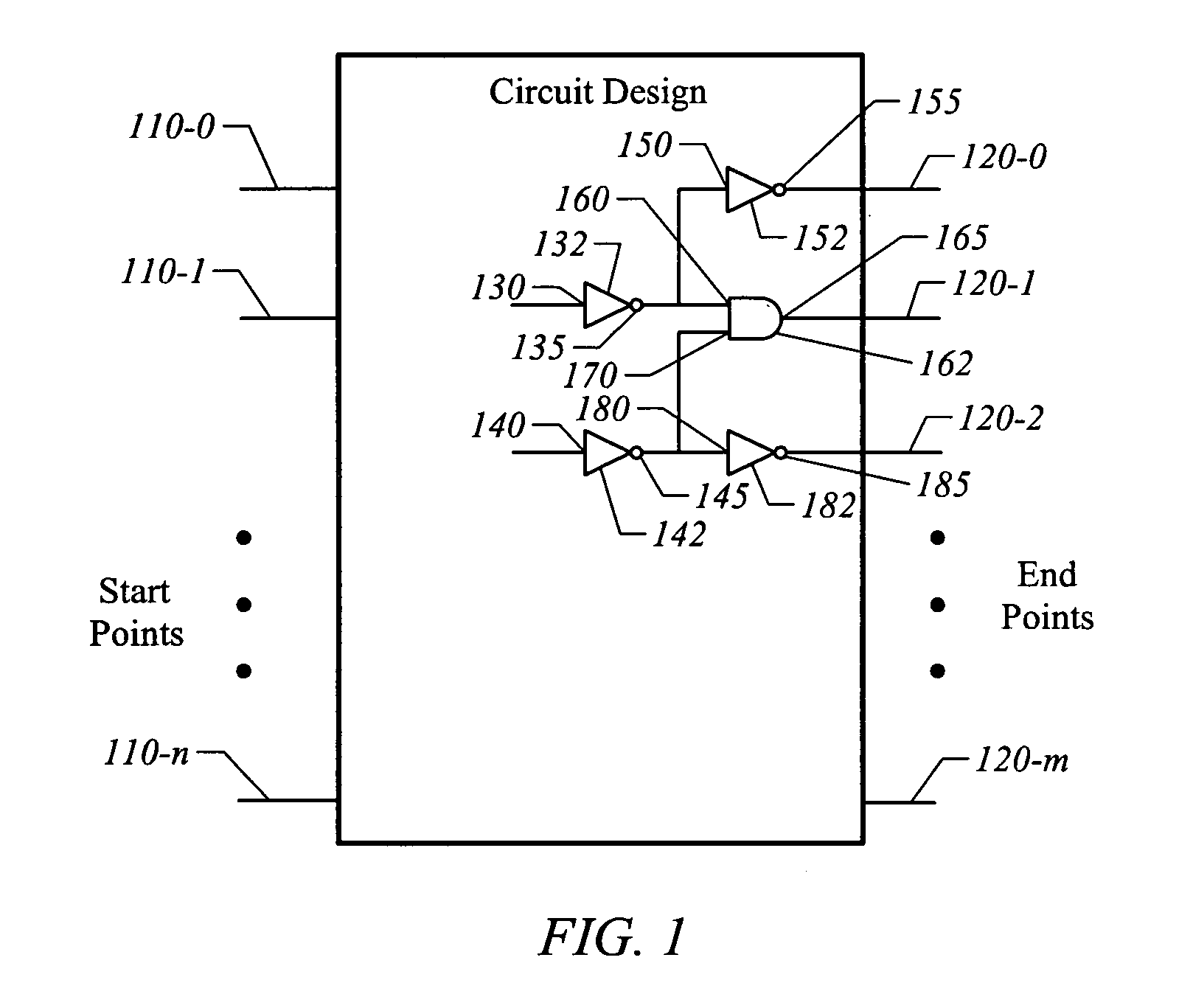
[0022]The goal of physical synthesis optimization engines is to optimize multiple objectives—timing, slew, capacitance, leakage, etc. The goal of any optimizer is to improve the paths between some predefined start points and end points. Any path in the circuit graph has a constraint for the time that is allocated for a signal to reach the end point from a start point. The goal of the optimization phase is to reduce the time required for the signal to travel ...
PUM
 Abstract
Description
Claims
Application Information