
Nonvolatile memory and method of address management

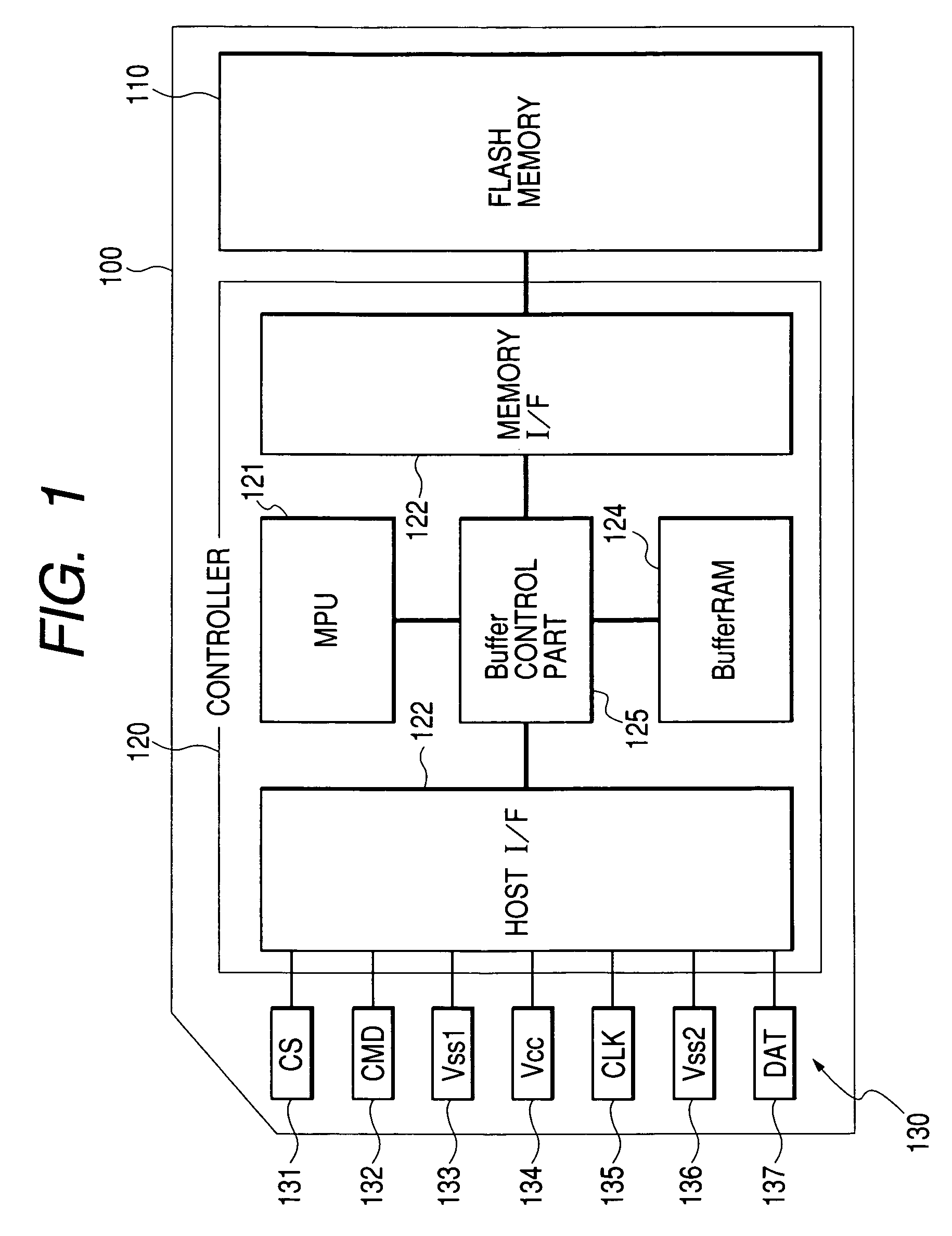
a memory and address technology, applied in the field of nonvolatile memory and address management, can solve the problems of multi-bank method problems, parallel writing among plural banks will not be possible, etc., and achieve the effects of increasing access time, slowing down access speed, and increasing memory such as external ram for expanding the reference tabl

Active Publication Date: 2007-03-27
RENESAS ELECTRONICS CORP
View PDF10 Cites 6 Cited by
  • Summary
  • Abstract
  • Description
  • Claims
  • Application Information

AI Technical Summary

Benefits of technology

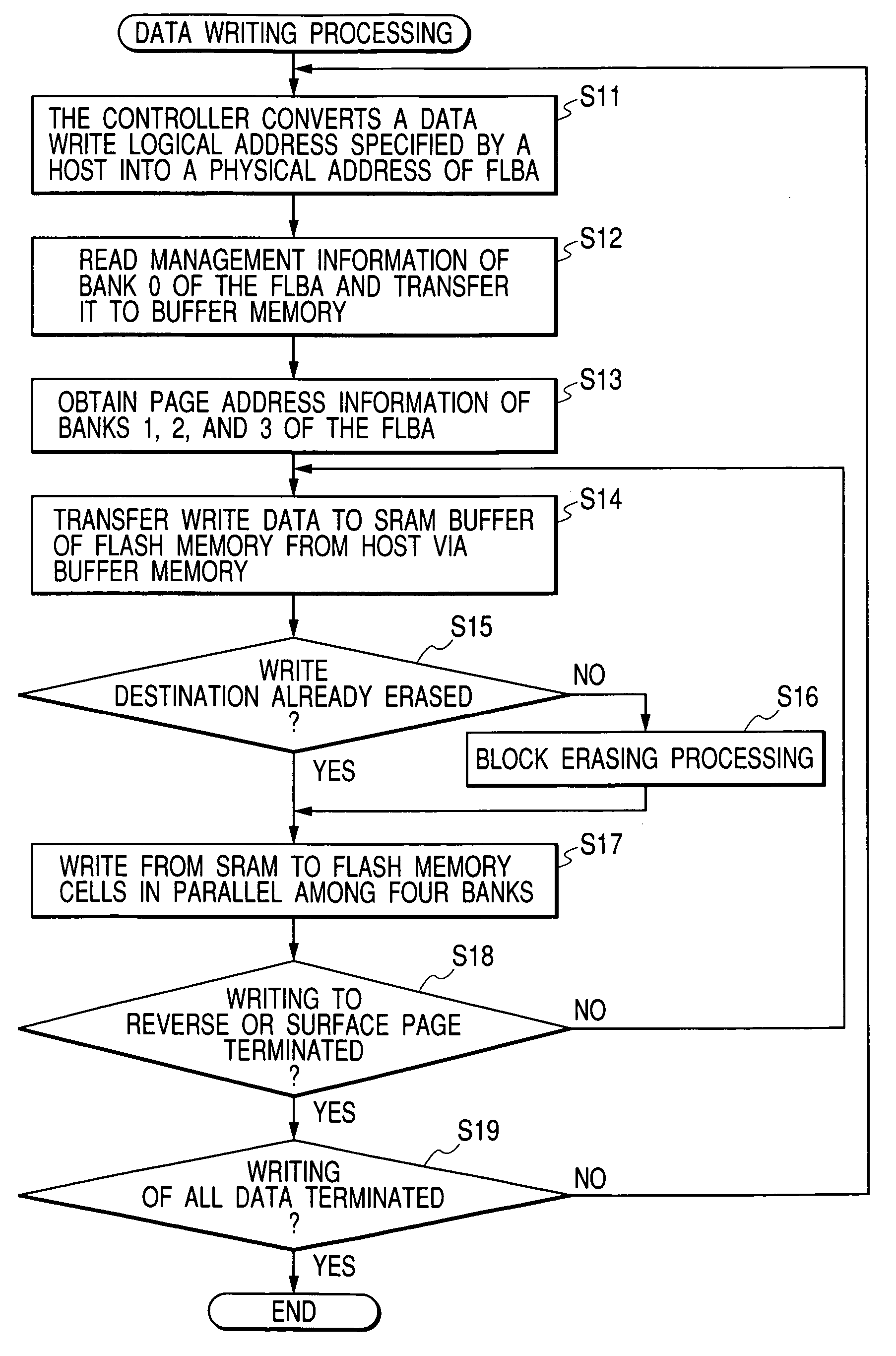
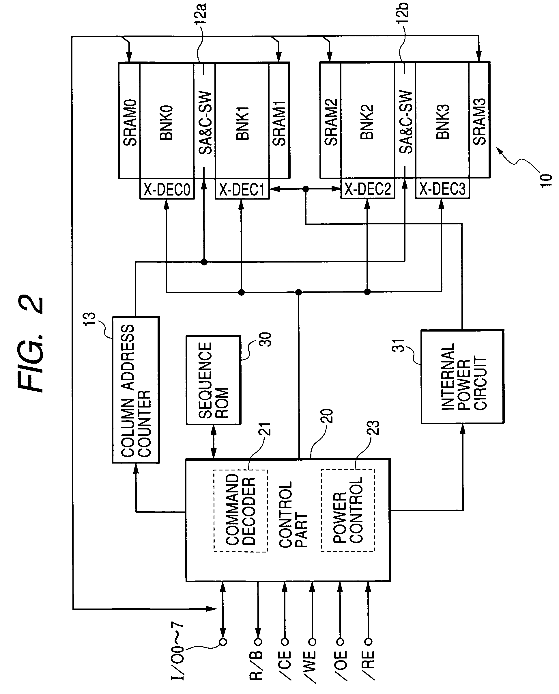
[0009]If a flash memory having four banks is managed by such a block-based address method, parallel writing among plural banks will be unable to be performed. Accordingly, as shown in FIG. 16, four buffer memories BFM0 to BFM3 comprising SRAM or the like are provided correspondingly to four banks BANK0 to BANK3, and identical blocks of different banks are coupled (grouped) so as to be associated with one address, thereby enabling parallel writing among plural banks.
[0014]If the amount of data of the reference table increases, since the reference table is generally stored within the flash memory, there arises a problem that an area available to users within the flash memory reduces, and the capacity of memory such as external RAM for expanding the reference table increases. The reference table is expanded in an external memory because frequent references to the reference table within the flash memory would make access time longer because the flash memory is slower in access speed than RAM.
[0015]An object of the present invention is to provide an address management method which makes it possible to prevent reduction in a substantial storage capacity due to an increase in the number of blocks that contain no defective bits but are not used in a memory system that uses an electrically writable and erasable nonvolatile semiconductor storage device having plural banks, such as flash memory.
[0016]Another object of the present invention is to provide an address management method which makes it possible to prevent reduction in a substantial storage capacity by decreasing the amount of data of a reference table for address translation in a memory system that uses an electrically writable and erasable nonvolatile semiconductor storage device having plural banks, such as flash memory, and adopts the table method.
[0017]Still another object of the present invention is to provide an address management method which makes it possible to reduce a storage capacity of external memory in a memory system that uses an electrically writable and erasable nonvolatile semiconductor storage device having plural banks, such as flash memory.
[0021]According to the above-described means, since chains of blocks containing no defective bits are formed, the number of blocks that contain no defective bits but are not used can be reduced.

Problems solved by technology

As a result, it became obvious that the multi-bank method has problems as described below.
If a flash memory having four banks is managed by such a block-based address method, parallel writing among plural banks will be unable to be performed.

Method used


Image

  • Nonvolatile memory and method of address management
  • Nonvolatile memory and method of address management
  • Nonvolatile memory and method of address management

Examples


second embodiment

[0088]FIG. 9 shows the configuration of inter-bank block chains of the flash memory in address management of a table method of the second embodiment and allocation examples of table areas.

first embodiment

[0089]The configuration of the inter-bank block chains is the same as that in the first embodiment described using FIG. 5A. In FIG. 9, each box marked with the symbol FLBA denotes a block consisting two pages, a surface page and a reverse page. Blocks belonging to different banks that are marked with identical symbols constitutes an identical inter-bank block chain. Hatched blocks contain defective bits.

[0090]As shown in FIG. 9, also in this embodiment, blocks are sequentially selected and grouped one at a time to form chains from the start of each bank except blocks containing defective bits, and addresses are sequentially assigned to the chains from the start thereof until the last block of any one bank is reached.

[0091]Furthermore, in the second embodiment, a specific portion of the memory array in which the chains are formed as described above is selected as a table storage area TSA, the specific portion having less blocks containing defective bits, and remaining areas are used ...


PUM


Abstract

A nonvolatile memory has plural memory blocks, each having a plurality of sub memory blocks, and is capable of programming to a first sub memory block within a first memory block and a second sub memory block within a second memory block in parallel. The first sub memory block has a management area for storing a management information including linking information between the first sub memory block corresponding sub memory blocks of other memory blocks. A control circuit controls reading the linking information from the first sub memory block in accordance with address information, and programming to the first sub memory block in accordance with the address information and corresponding sub memory blocks by the linking information.

Description

BACKGROUND OF THE INVENTION[0001]The present invention relates to technology effectively applied to an address management method in an electrically writable and erasable nonvolatile semiconductor storage device. Still, the present invention relates to technology effectively applied to a storage device such as, e.g., a memory card incorporating a flash memory having plural banks from which data can be erased collectively in a predetermined unit.[0002]Recently, as data storage media of portable electronic equipment such as digital cameras, card-type storage devices called memory cards have become widely used. The memory cards incorporate a nonvolatile memory such as a flash memory capable of holding stored data even if power is turned off. Most of the memory cards generally incorporate a nonvolatile memory and a controller to control the writing and reading of data to and from the nonvolatile memory.[0003]A flash memory incorporated in conventional memory cards, which generally has on...

Claims


Application Information

Patent Timeline
Patent Type & Authority Patents(United States)
IPC IPC(8): G06F12/00G06F12/16G06F12/02G06K19/07G11C16/02G11C16/10G11C29/04
CPCG06F12/0246G11C16/102
Inventor ASARI, SHINSUKETAMURA, TAKAYUKISHIRAISHI, ATSUSHI
Owner RENESAS ELECTRONICS CORP
Learn More