
Amplifier; and transmitter and communication device incorporating the same

a technology of amplifiers and amplifiers, applied in the field of amplifiers, can solve the problems of deteriorating communication quality, distorted output modulated signal, and inaccurate amplitude information of envelope eo(t), and achieve the effect of wide dynamic range, high gain, and wide dynamic rang

Active Publication Date: 2007-04-03
PANASONIC CORP
View PDF8 Cites 17 Cited by
  • Summary
  • Abstract
  • Description
  • Claims
  • Application Information

AI Technical Summary

Benefits of technology

[0047]According to the present invention, even in the case of an amplifier for transmission signals that employs a “large-sized” transistor, the impedance between the base and collector can be increased at its transmission frequency. As a result, power feedback at the time of transmission is suppressed, whereby a high gain can be obtained. Furthermore, there are provided an amplifier, a transmitter, and a communication device which are small-sized and inexpensive and which make it possible to obtain a uniform gain over a wide frequency range and improve the dynamic range of a power amplifier.
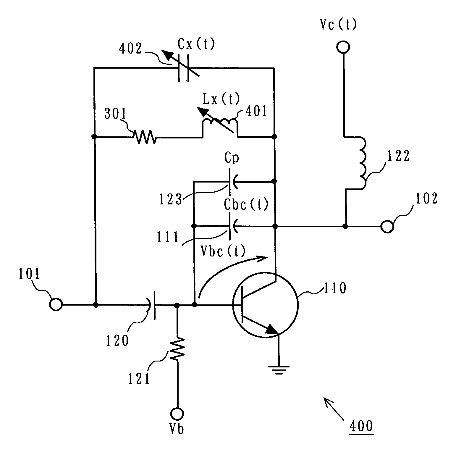
[0049]By connecting a capacitor in parallel with the inductor, the inductor can be downsized, whereby a small-sized amplifier can be provided. By allowing the capacitance of the capacitor to vary, it becomes possible to provide an amplifier which always has a high gain even in the case where the intrinsic capacitor fluctuates with time.
[0050]By allowing the inductance of the inductor to vary, it becomes possible to provide an amplifier which always has a high gain even in the case where the intrinsic capacitor fluctuates with time.
[0052]By allowing the transistor to operate in the saturation region, the power added efficiency can be enhanced.
[0053]In the case where the amplifier according to the present invention is employed for a transmitter capable of performing a polar coordinate modulation, an amplitude modulation signal only needs to be input to its last-stage amplifier. As a result, a wide dynamic range can be maintained even with a high modulation speed.

Problems solved by technology

Therefore, the output modulated signal is distorted, i.e., the envelope Eo(t) has inaccurate amplitude information.
This results in a deteriorated communication quality.
As described above, the transmitter shown in FIG. 11 has a third problem of having a narrow dynamic range.
In addition, the transmitter shown in FIG. 11 has a fourth problem in that the dynamic range becomes even narrower as a higher modulation speed is used, for the following reason.

Method used


Image

  • Amplifier; and transmitter and communication device incorporating the same
  • Amplifier; and transmitter and communication device incorporating the same
  • Amplifier; and transmitter and communication device incorporating the same

Examples


first embodiment

[0074](First Embodiment)

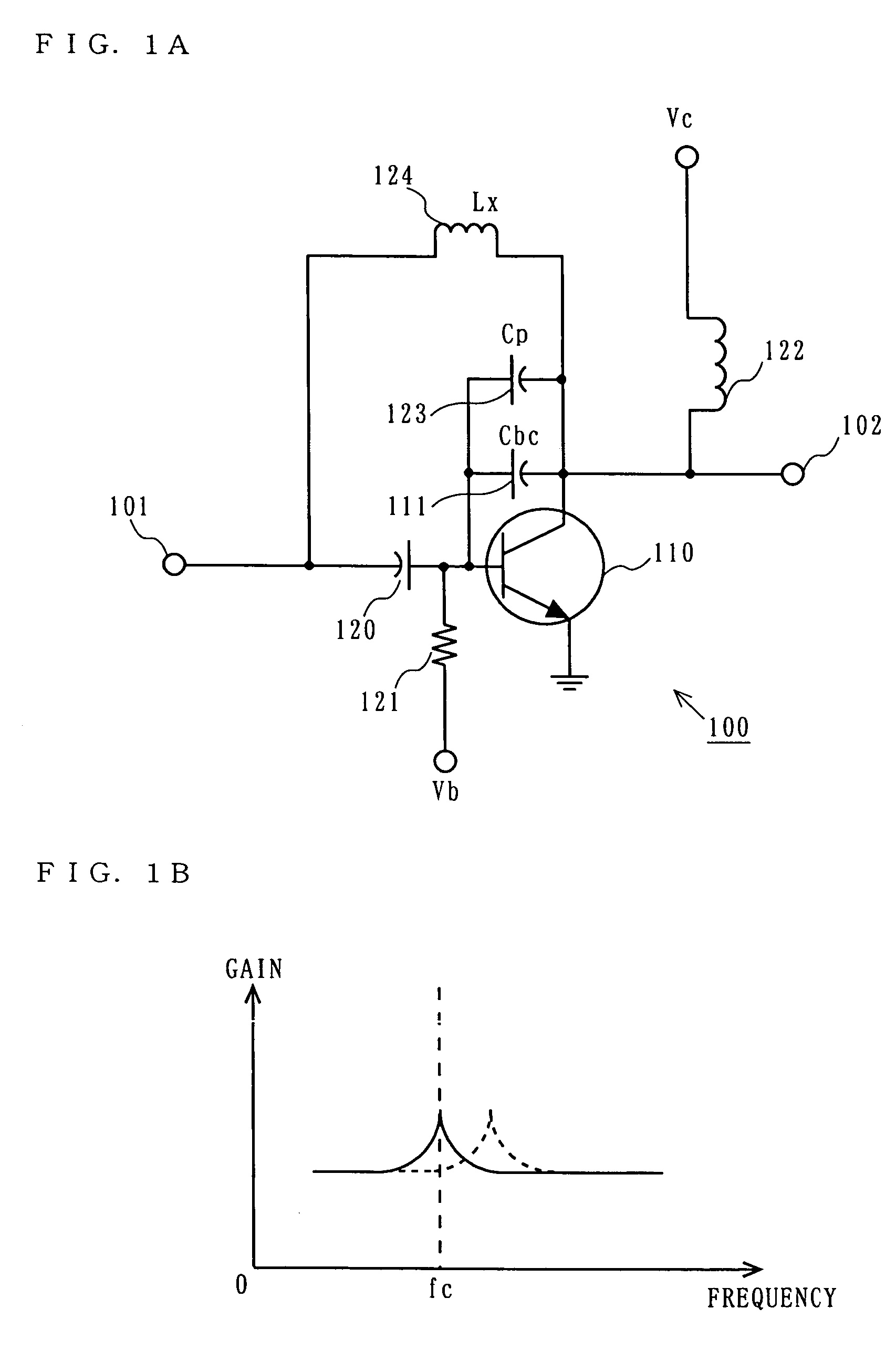
[0075]FIG. 1A is a circuit diagram illustrating the structure of an amplifier 100 according to a first embodiment of the present invention. As shown in FIG. 1A, the amplifier 100 comprises an input terminal 101, an output terminal 102, a transistor 110, a coupling capacitor 120, a resistor 121, an inductor 122, and an inductor 124.

[0076]In the amplifier 100 shown in FIG. 1A, a high-frequency signal which is input via a terminal 101 is applied to a base of a transistor 10. The signal is amplified, led through a collector, and taken out at an output terminal 102 as a transmission signal. To the base, a bias Vb is applied via a resistor 121. To the collector, a bias Vc is applied via an inductor 122.

[0077]Between the base and the collector of the transistor 110, a parasitic capacitor 123 and an intrinsic capacitor 111 are provided in a parallel connection. Furthermore, between the base and collector of the transistor 110, an inductor 124 (having an inductance Lx...

second embodiment

[0082](Second Embodiment)

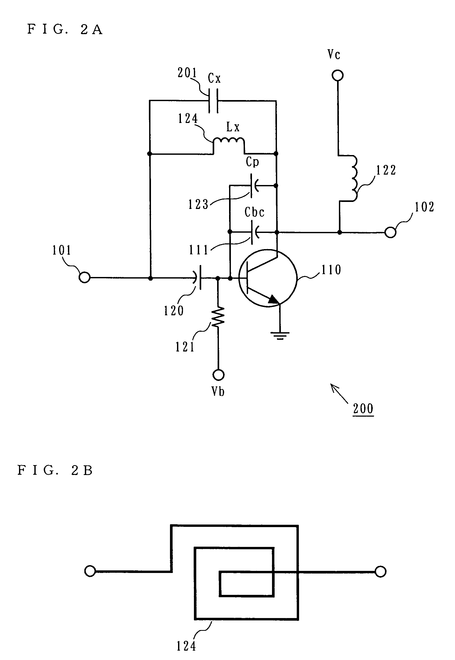
[0083]FIG. 2A is a circuit diagram illustrating the structure of an amplifier 200 according to a second embodiment of the present invention. The amplifier 200 shown in FIG. 2A is similar in construction to the amplifier 100 according to the first embodiment except that a further capacitor 201 (having a capacitance Cx) is connected between the base and collector.

[0084]Since the capacitor 201 is in a parallel connection with the parasitic capacitor 123 (having a capacitance Cp) and the intrinsic capacitor 111 (having a capacitance Cbc), the overall capacitance value is increased. Therefore, the value of the reactance Lx which satisfies the relationship of eq. 3 below can be smaller than that which satisfies the relationship of eq. 2:

Lx×(Cbc+Cp+Cx)=1 / ω2  eq. 3.

[0085]The physical size of the inductor can be more reduced as the value of LX decreases. Therefore, according to the second embodiment, by using an inductor 124 having a reactance Lx which satisfies the ...

third embodiment

[0087](Third Embodiment)

[0088]FIG. 3A is a circuit diagram illustrating the structure of an amplifier 300 according to a third embodiment of the present invention. FIG. 3B is a graph showing the frequency characteristics of the gain of the amplifier 300. The amplifier 300 shown in FIG. 3A is similar in construction to the amplifier 200 shown in FIG. 2A, except that a resistor 301 is connected in series with the inductor 124.

[0089]In the amplifier 300, if a parallel resonance circuit 302 which is composed of the parasitic capacitor 123 (having a capacitance Cp), the intrinsic capacitor 111 (having a capacitance Cbc), the inductor 124 (reactance Lx), and the capacitor 201 (having a capacitance Cx) did not have a resistance component, the parallel resonance circuit 302 would have a very large Q value, so that steep changes in impedance would occur along the frequency axis. In order to obtain a uniform gain in a communication band from f1 to f2, for example, such steep changes in the re...


PUM


Abstract

The present invention provides an amplifier for amplifying a high-frequency signal and outputting an amplified signal. The amplifier includes: an amplification element which is a bipolar transistor or a field-effect transistor; and an inductor connected between a base and a collector or between a gate and a drain of the amplification element. The inductance of the inductor is chosen so that, within a predetermined frequency range, a parallel resonance occurs with a parasitic capacitor of the amplification element and an intrinsic capacitor of the amplification element, the intrinsic capacitor being a base-collector capacitance or a gate-drain capacitance.

Description

BACKGROUND OF THE INVENTION[0001]1. Field of the Invention[0002]The present invention relates to an amplifier as well as a transmitter and a communication device incorporating the same. More particularly, the present invention relates to an amplifier which operates with a high frequency, as well as a transmitter and a communication device incorporating the same.[0003]2. Description of the Background Art[0004]A power amplifier to be used in a transmission block of a mobile phone or the like must be able to amplify a signal on the order of several W with a high gain.[0005]FIG. 10 is a diagram illustrating an exemplary structure of a conventional amplifier 900 designed for amplifying a weak received signal (see, for example, Behzad Razavi, “RF Microelectronics”, Prentice-Hall, Nov. 1, 1997, p.169).[0006]In the amplifier 900 shown in FIG. 10, a signal which is input via a terminal 901 is applied to a base of a transistor 910. The signal is amplified, led through a collector, and taken o...

Claims


Application Information

Patent Timeline
Patent Type & Authority Patents(United States)
IPC IPC(8): G06G7/12H03F1/34H03F3/19
CPCH03F3/19H03F2200/138
Inventor MORIMOTO, SHIGERUADACHI, HISASHI
Owner PANASONIC CORP
Learn More