Mesa isolation technology for extremely thin silicon-on-insulator semiconductor devices

a silicon-on-insulator, extremely thin technology, applied in the direction of semiconductor devices, electrical devices, transistors, etc., can solve the problems of poor breakdown performance, high manufacturing cost, and high manufacturing cost of sti techniques, so as to improve electrical characteristics and efficient manufacturing

Active Publication Date: 2007-04-10
ADVANCED MICRO DEVICES INC
View PDF17 Cites 48 Cited by
  • Summary
  • Abstract
  • Description
  • Claims
  • Application Information

AI Technical Summary

Benefits of technology

[0014]This invention addresses the needs for an efficiently-manufactured,

Problems solved by technology

Shallow junctions are necessary to avoid lateral diffusion of implanted dopants into the channel, since such diffusion disadvantageously contributes to leakage currents and poor breakdown performance.
STI techniques significantly increase manufacturing cost because the STI process consists of a number of processing steps and apparatuses, such as

Method used


Image

  • Mesa isolation technology for extremely thin silicon-on-insulator semiconductor devices
  • Mesa isolation technology for extremely thin silicon-on-insulator semiconductor devices
  • Mesa isolation technology for extremely thin silicon-on-insulator semiconductor devices

Examples


Embodiment Construction

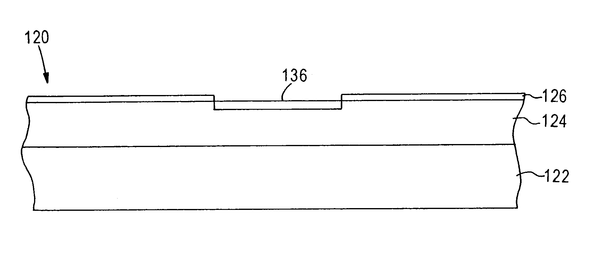
[0021]The present invention enables the production of improved high-speed semiconductor devices with the benefits of ETSOI technology. The present invention further provides the manufacturing efficiencies provided by mesa isolation fabrication techniques. In addition, the present invention reduces the SOI semiconductor device current leakage through exposed silicon layer sidewalls.

[0022]The invention will be described in conjunction with the formation of the ETSOI semiconductor devices illustrated in the accompanying drawings. However, these are exemplary only as the claimed invention is not limited to the formation of the specific devices illustrated in the drawings.

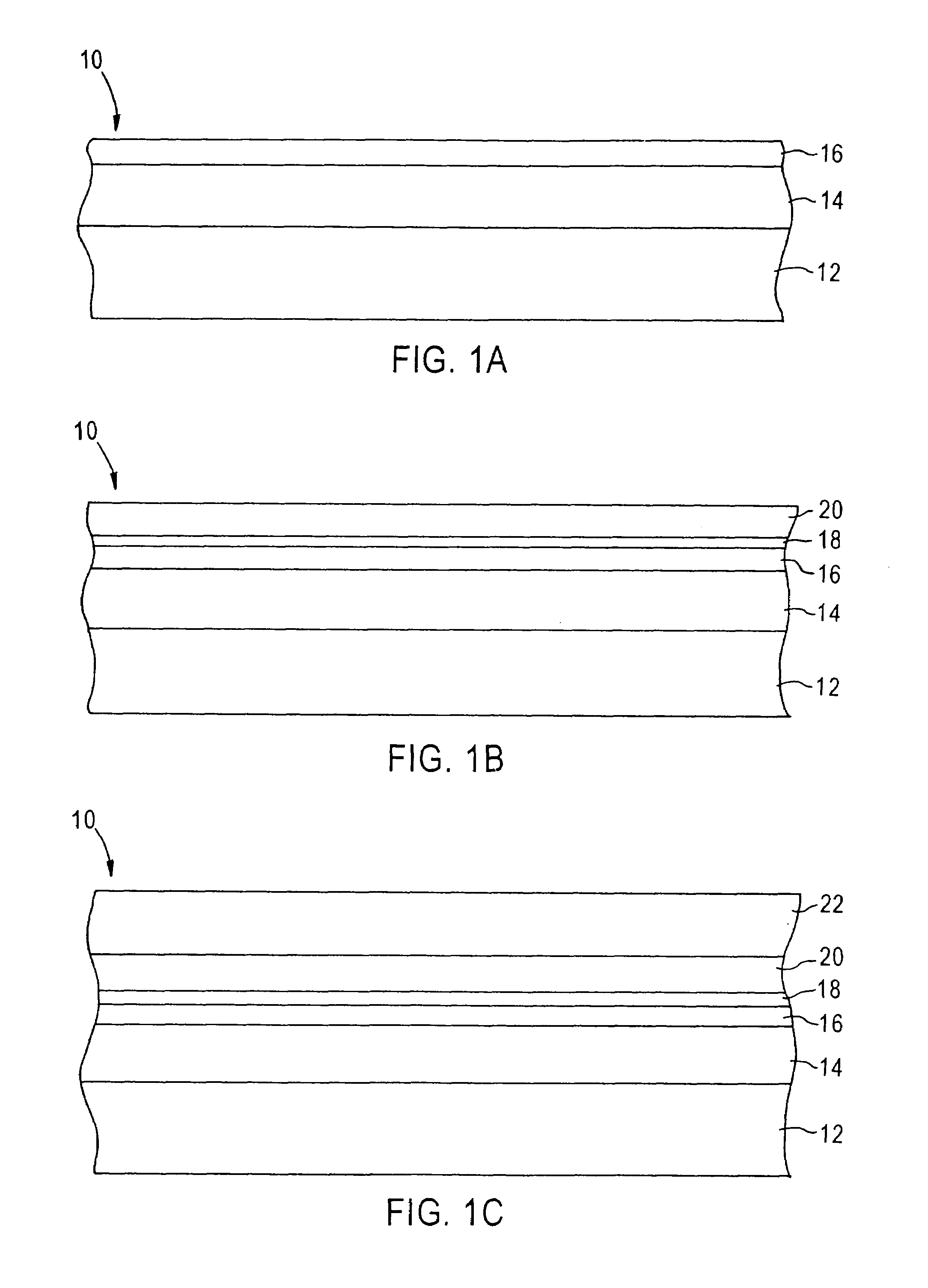
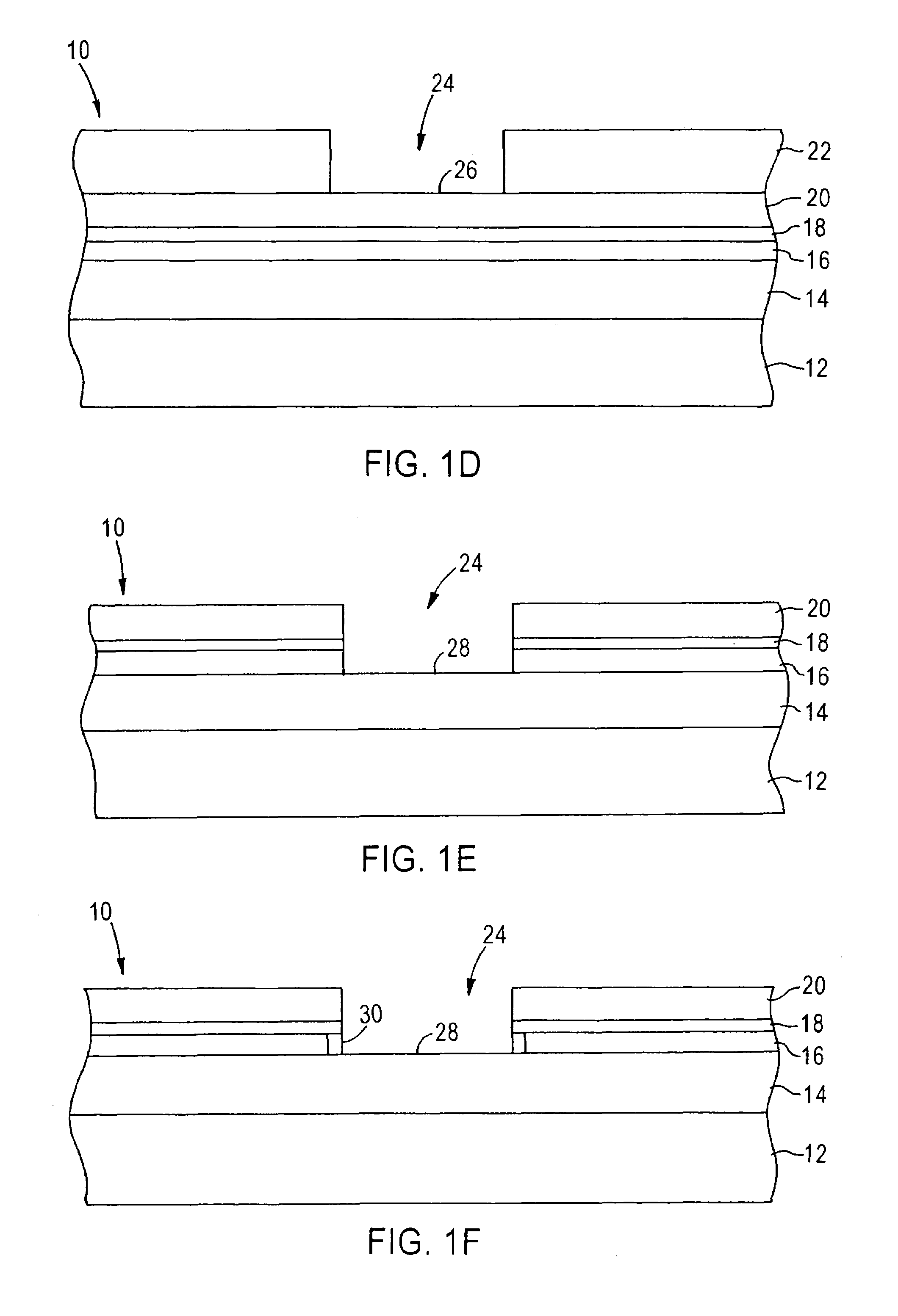
[0023]Typically, thin SOI semiconductor devices use shallow trench isolation (STI) techniques to electrically isolate adjacent semiconductor devices formed on a common substrate. A typical STI technique will be described. A SOI structure 10 is provided with a silicon layer 16 and an insulating layer 14 overlying a subst...


PUM


Abstract

Silicon-on-insulator (SOI) structures with silicon layers less than 20 nm in thickness are used to form extremely thin silicon-on-insulator (ETSOI) semiconductor devices. ETSOI semiconductor devices can be efficiently manufactured by mesa isolation techniques. A method of forming a plurality of semiconductor devices is provided comprising a SOI structure. The SOI structure comprises a substrate, an insulating layer overlying the substrate, and a silicon layer overlying the insulating layer, wherein the silicon layer has a thickness less than 20 nm. The silicon layer is patterned to create at least two laterally spaced apart silicon layers. A semiconductor device is formed at each of the at least two laterally spaced apart silicon layers.

Description

FIELD OF THE INVENTION[0001]The present invention relates to semiconductor devices and methods of manufacturing semiconductor devices and, more particularly, to an improved semiconductor device comprising silicon-on-insulator (SOI) technology.BACKGROUND OF THE INVENTION[0002]An important aim of ongoing research in the semiconductor industry is increasing semiconductor performance while decreasing power consumption in semiconductor devices. Planar transistors, such as metal oxide semiconductor field effect transistors (MOSFETs) are particularly well suited for use in high-density integrated circuits. As the size of MOSFETs and other devices decrease, the dimensions of source / drain regions, channel regions, and gate electrodes of the devices, also decrease.[0003]The design of ever-smaller planar transistors with short channel lengths makes it necessary to provide very shallow source / drain junctions. Shallow junctions are necessary to avoid lateral diffusion of implanted dopants into t...

Claims


Application Information

Patent Timeline
IPC IPC(8): H01L21/336
CPCH01L21/26506H01L29/6659H01L29/7833
Inventor PAN, JAMES
Owner ADVANCED MICRO DEVICES INC
Why Eureka
Try Eureka