
Silica thin films produced by rapid surface catalyzed vapor deposition (RVD) using a nucleation layer

a technology of surface catalysis and thin films, applied in chemical vapor deposition coatings, coatings, metallic material coating processes, etc., can solve the problems of increasing the depth to width of features, the deposition rate is very low, and the traditional cvd technique cannot provide adequate conformal films in these high aspect ratio features

Active Publication Date: 2007-04-10
NOVELLUS SYSTEMS
View PDF59 Cites 45 Cited by
  • Summary
  • Abstract
  • Description
  • Claims
  • Application Information

AI Technical Summary

Benefits of technology

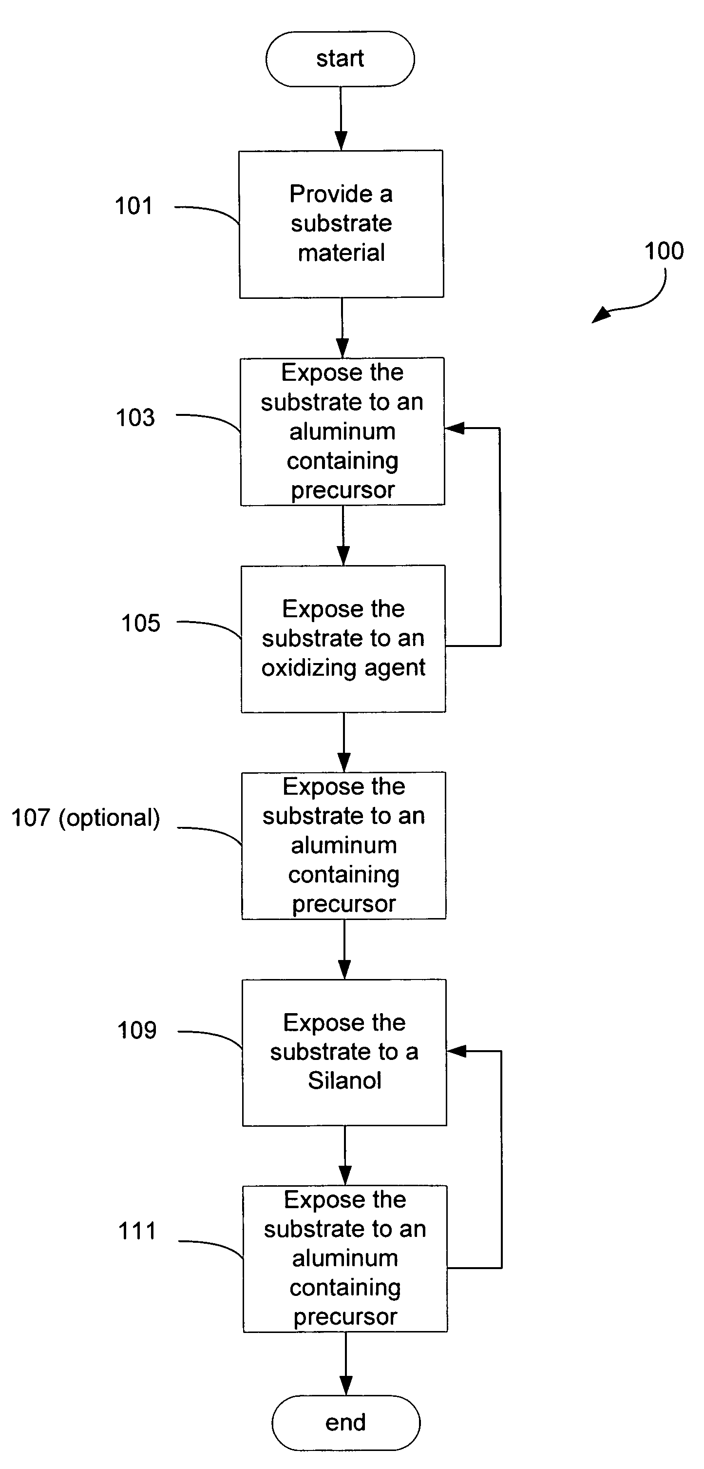
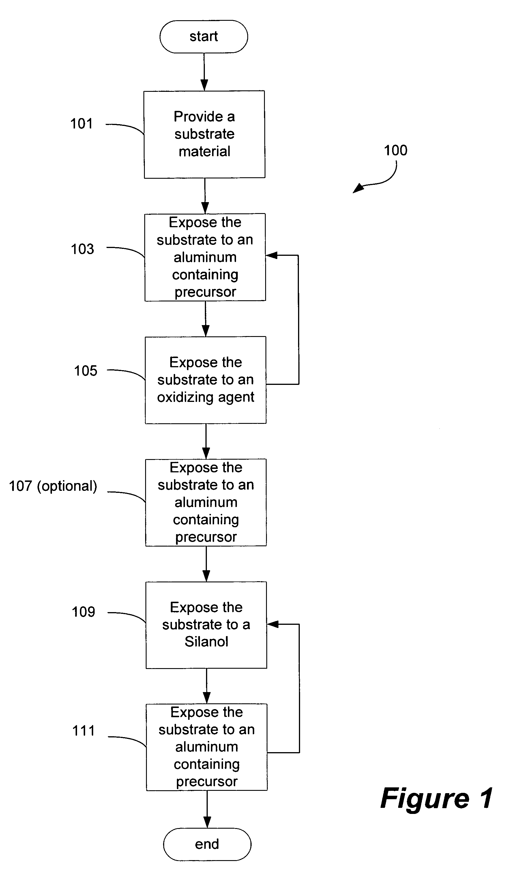
[0009]The present invention provides a method for using ALD and RVD techniques to produce a smooth dielectric film. This method involves three principal operations: 1) exposing the substrate surface with an aluminum-containing precursor to form a substantially saturated surface of aluminum-containing precursor and 2) exposing the substrate surface to an oxygen-containing oxidizer; and 3) exposing the substrate surface to a silicon-containing precursor. In variations of the invention, operations 1) and 2) are repeated a number of times, for example a total of 2–5 times, prior to operation 3). Alternately, up to about ten iterations of operations 1) and 2) may be applied. In a preferred embodiment of the invention, following one or more iterations of operations 1) and 2), generally from 2–5, an aluminum-containing precursor is again formed on the substrate surface prior to operation 3). Alternately, any suitable metal-containing precursor that can sufficiently absorb onto the substrate surface and sufficiently react with the subsequently added silicon-containing precursor to form a dielectric layer that is more than a monolayer thick may be used in place of the aluminum-containing precursor. Other metal-containing precursors that can be deposited to reactivate the catalytic surface include, but are not limited to, zirconium, hafnium, gallium, titanium, niobium, tantalum, and their oxides or nitrides.

Problems solved by technology

However as design rules continue to shrink, the aspect ratios (depth to width) of features increase, and traditional CVD techniques can no longer provide adequately conformal films in these high aspect ratio features.
One drawback, however, to ALD is that the deposition rates are very low.
These processes are unacceptably slow in some applications in the manufacturing environment.
However, the first cycle is often rough and non-uniform due to poor nucleation on the substrate.
This poor nucleation can translate into as much as 33% variation in film thickness across the wafer and within the features to be filled, and can dramatically increase the surface roughness.
This additional surface roughness can, among other problems, decrease precursor utilization by limiting precursor flux to the bottom of the filled trenches (i.e., a smooth-walled trench will fill up more efficiently than one with rough walls.)

Method used


Image

  • Silica thin films produced by rapid surface catalyzed vapor deposition (RVD) using a nucleation layer
  • Silica thin films produced by rapid surface catalyzed vapor deposition (RVD) using a nucleation layer
  • Silica thin films produced by rapid surface catalyzed vapor deposition (RVD) using a nucleation layer

Examples


examples

[0046]The following examples provide details concerning the implementation of an embodiment of the present invention and beneficial results. It should be understood the following is representative only, and that the invention is not limited by the detail set forth in these examples.

[0047]In one example of a preferred embodiment, an Al2O3 nucleation layer was deposited over a high aspect ratio feature (i.e., a trench) on a substrate by placing a substrate material (i.e., a silicon wafer), in a reaction chamber and then exposing the substrate to tri-methyl-aluminum for one second. This was followed by a five-second reactor purge, wherein an inert gas was introduced into the reaction chamber. Next, the substrate was exposed to water, an oxidizer, by opening a valve separating a container with water vapor at 24 Torr and 25° C. for one second. The process was repeated for four cycles, followed by a half cycle (just the tri-methyl-aluminum deposition) before the application of a silica la...


PUM

PropertyMeasurementUnit
temperaturesaaaaaaaaaa
pressuresaaaaaaaaaa

Abstract

An method employing atomic layer deposition (ALD) and rapid vapor deposition (RVD) techniques conformally deposits a dielectric material on small features of a substrate surface. The resulting dielectric film has a low dielectric constant and a high degree of surface smoothness. The method includes the following three principal operations: exposing a substrate surface to an aluminum-containing precursor gas to form a saturated layer of aluminum-containing precursor on the substrate surface; exposing the substrate surface to an oxygen-containing gas to oxidize the layer of aluminum-containing precursor; and exposing the substrate surface to a silicon-containing precursor gas to form the dielectric film. Generally an inert gas purge is employed between the introduction of reactant gases to remove byproducts and unused reactants. These operations can be repeated to deposit multiple layers of dielectric material until a desired dielectric thickness is achieved.

Description

FIELD OF THE INVENTION[0001]This invention pertains to methods for forming thin dielectric films. More specifically, the invention pertains to methods of depositing a conformal film of dielectric material on a semiconductor device with a high degree of surface smoothness.BACKGROUND OF THE INVENTION[0002]Conformal, uniform dielectric films have many applications in semiconductor manufacturing. In the fabrication of sub-micron integrated circuits (ICs) several layers of dielectric film are deposited. Four such layers are shallow trench isolation (STI), premetal dielectric (PMD), inter-metal dielectric (IMD) and interlayer dielectric (ILD). All four of these layers require silicon dioxide films that fill features of various sizes and have uniform film thicknesses across the wafer.[0003]Chemical vapor deposition (CVD) has traditionally been the method of choice for depositing conformal silicon dioxide films. However as design rules continue to shrink, the aspect ratios (depth to width) ...

Claims


Application Information

Patent Timeline
Patent Type & Authority Patents(United States)
IPC IPC(8): H01L21/31H01L21/469
CPCC23C16/0272C23C16/402C23C16/45525C23C16/45534H01L21/02145H01L21/02164H01L21/02178H01L21/0228H01L21/3141H01L21/31612
Inventor HAUSMANN, DENNIS M.TOBIN, JEFFPAPASOULIOTIS, GEORGE D.RULKENS, RONTARAFDAR, RAIHAN M.TIPTON, ADRIANNE K.NIE, BUNSEN
Owner NOVELLUS SYSTEMS
Learn More