
Method of forming metal silicide

a metal silicide and metal silicide technology, applied in the direction of semiconductor devices, electrical equipment, basic electric elements, etc., can solve the problems of source/drain region, low resistance of titanium silicide, and presenting risks, so as to reduce the instability of nickel silicide and achieve rapid thermal anneal

Active Publication Date: 2007-04-17
TAIWAN SEMICON MFG CO LTD
View PDF10 Cites 11 Cited by
  • Summary
  • Abstract
  • Description
  • Claims
  • Application Information

AI Technical Summary

Benefits of technology

This approach enables stable nickel silicide formation at temperatures below 750°C, preventing agglomeration and ensuring uniformity, thus enhancing MOSFET device performance by reducing silicon consumption and maintaining low resistance.

Problems solved by technology

The minimum resistance of titanium silicide is difficult to achieve sometimes necessitating several anneal cycles needed to obtain the low resistance C54 phase, specifically when titanium silicide is formed on the top surface of narrow width conductive gate structures.
In addition during the consumption of silicon during metal silicide formation greater silicon consumption is encountered during cobalt silicide formation than experienced with other metal silicide counterparts thus presenting risks when shallow source / drain regions are employed.
Nickel silicide features desirable low resistance as well as consuming only minimal amounts of silicon during formation, however the attainment of nickel silicide can be more difficult to achieve than other metal silicides such as titanium silicide or cobalt silicide.
Nickel silicide is unstable at temperatures greater than 750° C., sometimes resulting in an agglomeration phenomena, therefore an anneal procedure performed at these temperatures, applied to a nickel layer directly on a narrow width conductive gate structure can result in unwanted nickel silicide agglomeration.

Method used


Image

  • Method of forming metal silicide
  • Method of forming metal silicide
  • Method of forming metal silicide

Examples


Embodiment Construction

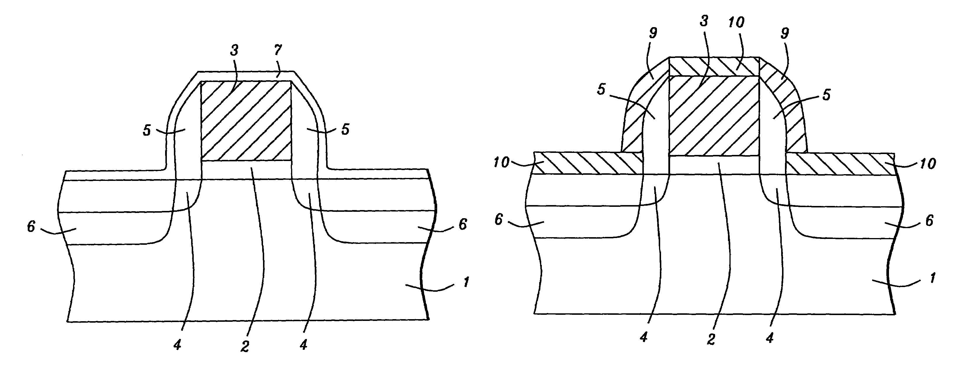
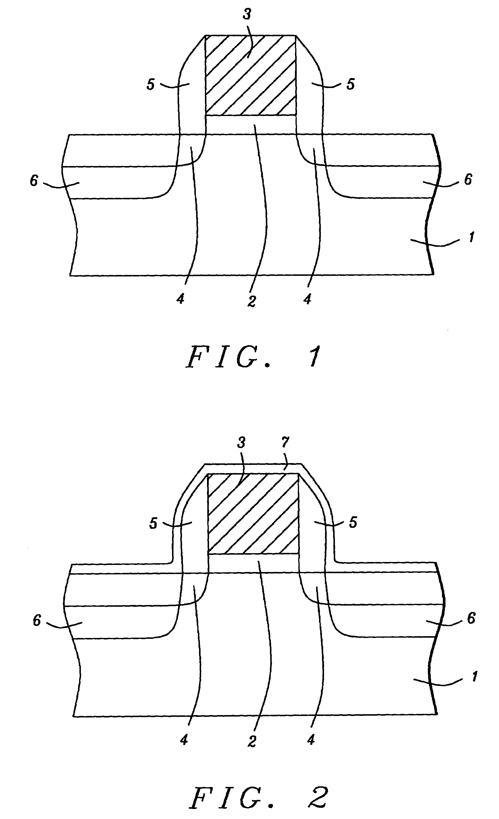
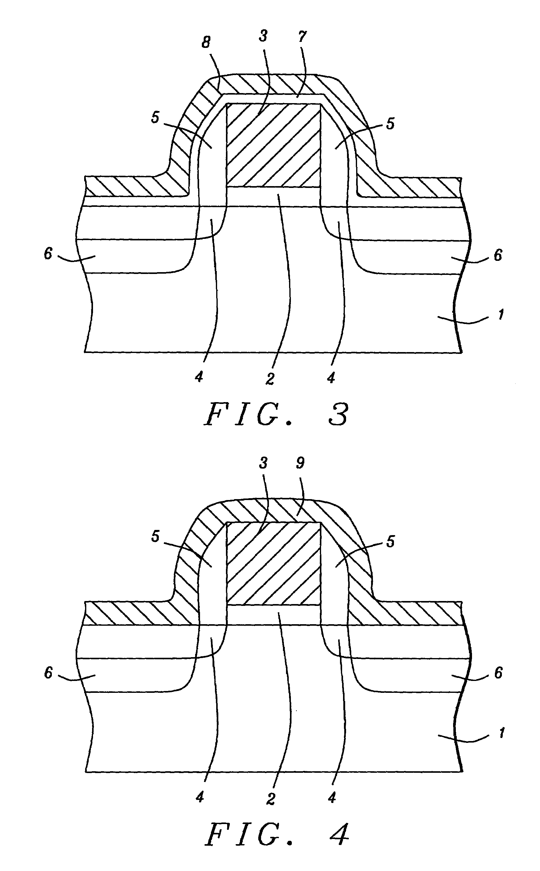
[0013]The method of forming nickel silicide on MOSFET device regions featuring a thin titanium interlayer, obtained via ALD procedures and employed to allow nickel silicide to be formed at temperatures in which nickel silicide instability is eliminated, will now be described in detail. This invention will be described for an N channel MOSFET device, however it should be understood that this invention can also be applied to a P channel MOSFET as well as to a complimentary (CMOS) device. FIG. 1, schematically shows the MOSFET device to which this invention will be applied. P type semiconductor substrate 1, comprised of single crystalline silicon featuring a crystallographic orientation is used. Gate insulator layer 2, comprised of silicon dioxide is thermally grown to a thickness between about 10 to 100 Angstroms. If desired a high dielectric constant (high k), layer, with a dielectric constant greater than 4, can be used as a gate insulator layer. Conductive gate structure 3, a stru...


PUM

PropertyMeasurementUnit
thicknessaaaaaaaaaa
thicknessaaaaaaaaaa
dielectric constantaaaaaaaaaa

Abstract

A method of optimizing the formation of nickel silicide on regions of a MOSFET structure, has been developed. The method features formation of nickel silicide using an anneal procedure performed at a temperature below which nickel silicide instability and agglomeration occurs. A thin titanium interlayer is first formed on the MOSFET structure prior to nickel deposition, allowing an anneal procedure, performed after nickel deposition, to successfully form nickel silicide at a temperature of about 400° C. To obtain the desired conformality and thickness uniformity the thin titanium interlayer is formed via an atomic layer deposition procedure.

Description

BACKGROUND OF THE INVENTION[0001](1) Field of the Invention[0002]The present invention relates to methods used to fabricate semiconductor devices and more specifically to a process used to form metal silicide on specific regions of metal oxide semiconductor field effect transistor (MOSFET) devices.[0003](2) Description of Prior Art[0004]To improve MOSFET device performance metal silicide has been used on source / drain as well as on conductive gate structures. The use of the lower resistance metal silicide, when compared to more resistive non-silicided source / drain regions and polysilicon gate structures, result in he desired resistance—capacitance (RC) values allowing MOSFET performance enhancement to be realized. Candidates for metal silicide include titanium silicide as well as cobalt silicide, however both present shortcomings when used for MOSFET devices that are comprised with shallow source / drain regions and narrow width gate structures. The minimum resistance of titanium silic...

Claims


Application Information

Patent Timeline
Patent Type & Authority Patents(United States)
IPC IPC(8): H01L21/44H01L21/28H01L21/285H01L21/3205H01L21/336H01L21/4763H01L21/8234H01L21/8238
CPCH01L21/28052H01L21/28518H01L29/665H01L21/823835
Inventor WU, CHII-MINGWANG, MEI-YUNCHANG, CHIH-WEISHUE, SHAU-LIN
Owner TAIWAN SEMICON MFG CO LTD
Learn More