

Image display apparatus
- Summary
- Abstract
- Description
- Claims
- Application Information
AI Technical Summary
Benefits of technology
Problems solved by technology
Method used
Image

Examples
second embodiment
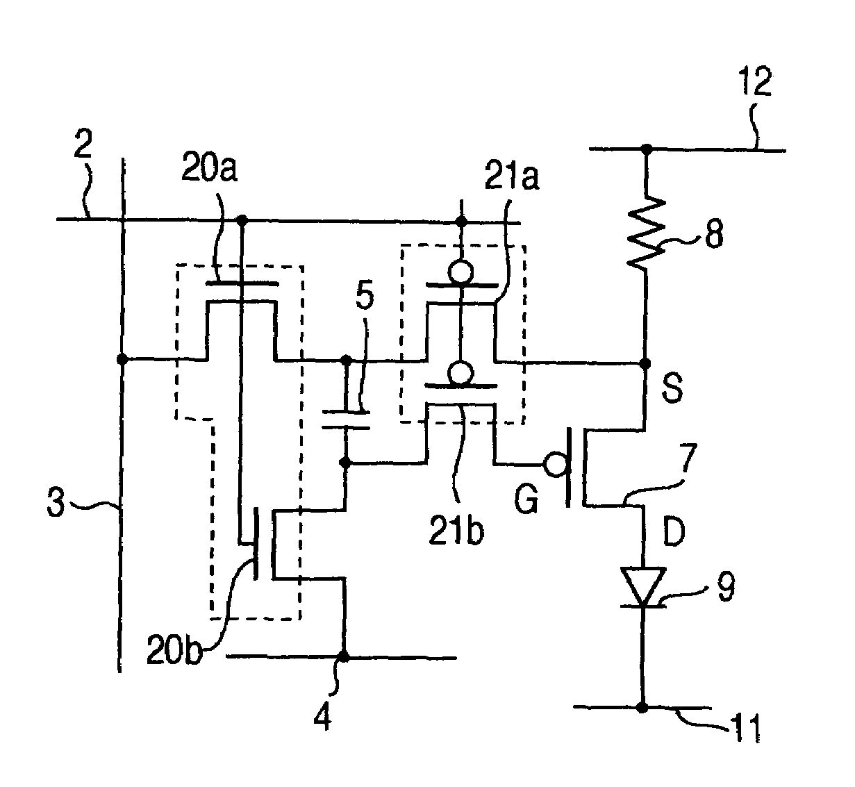
[0065]Next, a memory control circuit used in the present invention will be described with reference to FIG. 6.
[0066]In the second embodiment, the use of n-type thin film transistors (driving TFT) as driving elements is taken into consideration. Also, for using n-type thin film transistors for all elements, the sampling switch elements 20a, 20b and driving switch elements 21a, 21b are comprised of n-type thin film transistors. In this configuration, an inverted scanning signal wire 60 for transmitting an inverted scanning signal which has the opposite polarity to the scanning signal, is routed in parallel with the scanning wire 2 associated with each pixel in order, and each of the driving switches 21a, 21b has a gate connected to the inverted scanning signal wire 60 to complementarily drive the respective sampling switch elements 20a, 20b and the respective driving switch elements 21a, 21b. The remaining configuration is similar to that illustrated in FIG. 4.
[0067]In the second embo...
third embodiment
[0071]In the third embodiment, the driving TFT 7 has the gate directly connected to one end of the sampling capacitor 5, and a signal voltage during a sampling operation is held by a gate capacitance of the driving TFT 7, so that the number of required thin film transistors can be reduced by one from the aforementioned embodiments, leading to an improvement on the numerical aperture of the pixel.
fourth embodiment
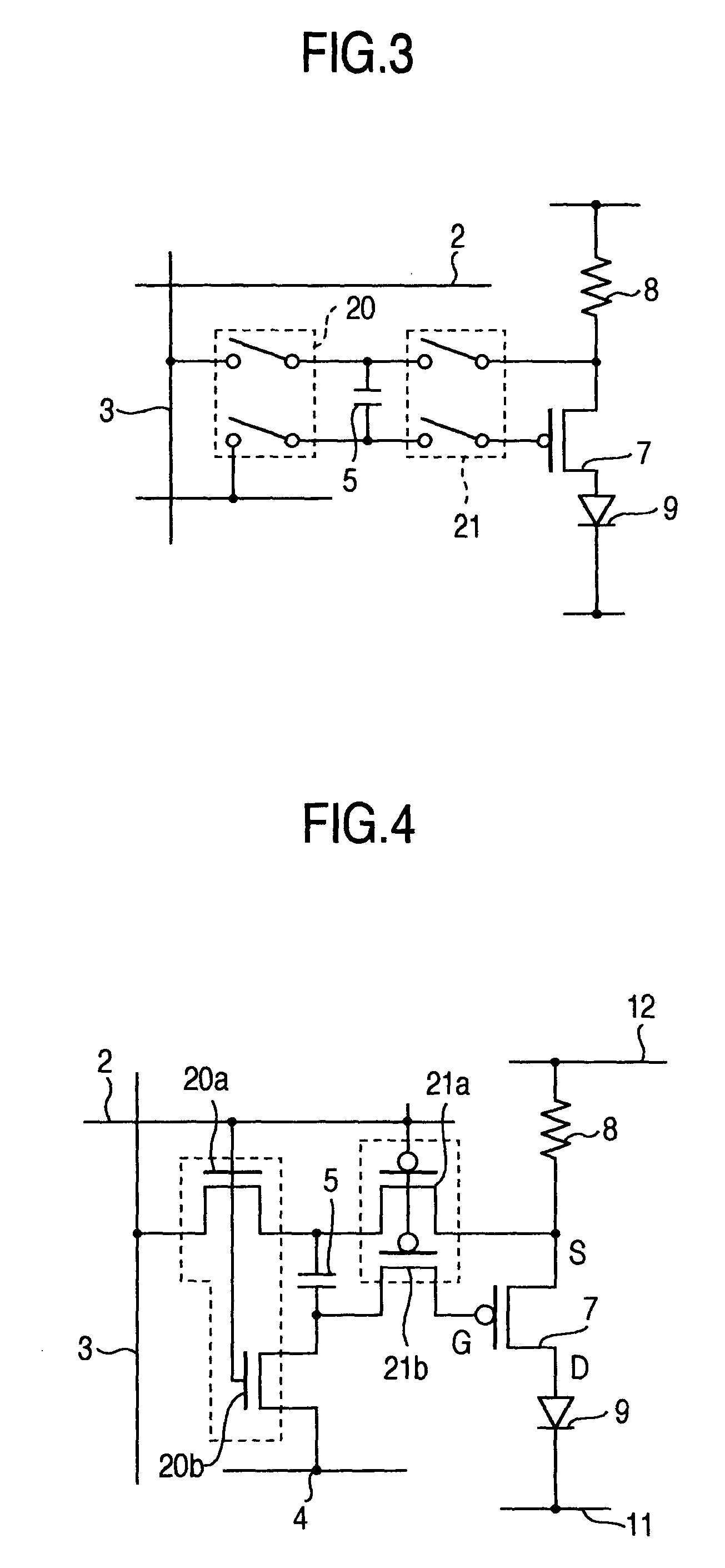
[0072]Next, the present invention will be described with reference to FIG. 8. This embodiment employs a memory circuit in place of the memory control circuit in each of the foregoing embodiments, and an n-type reference control TFT 81 inserted between the driving TFT 7 and organic LED 9 as a power supply control element. The remaining configuration is similar to that in the aforementioned respective embodiments.
[0073]The memory circuit comprises a sampling TFT 80 as a sampling switch element which becomes conductive in response to a source signal to sample a signal voltage; and a sampling capacitor 5 for holding the signal voltage sampled by the sampling TFT 80. The sampling TFT 80 is comprised of a n-type double-gate thin film transistor which has a gate connected to the scanning wire 2; a drain connected to the signal wire 3; and a source connected to the gate of the n-type driving TFT 7 and to one end of the sampling capacitor 5.
[0074]The sampling capacitor 5 has the other end co...
PUM
 Abstract
Description
Claims
Application Information