
Photonic crystal fiber preform and photonic crystal fiber manufactured using the same

a technology preform, which is applied in the field of photonic crystal fiber preform and photonic crystal fiber manufactured using the same, can solve the problems of limiting the design of photonic crystal fiber preform and the limited properties of the material constituting the core of the photonic crystal fiber, and achieves the effect of easy manufacturing and easy realization of optical fiber design

Active Publication Date: 2007-04-17
SAMSUNG ELECTRONICS CO LTD
View PDF20 Cites 0 Cited by
  • Summary
  • Abstract
  • Description
  • Claims
  • Application Information

AI Technical Summary

Benefits of technology

[0011]The present invention, which has been made in view of the above problems, provides, in one aspect, a photonic crystal fiber preform which is easily manufactured and makes it easy to realize design of optical fibers, and a photonic crystal fiber manufactured using the same.
[0012]In another aspect, the present invention is directed to a photonic crystal fiber preform which is capable of providing a single mode over a wide range of wavelengths and improving its transmission mode and its loss characteristics by simple design of a lattice structure thereof, and a photonic crystal fiber manufactured using the same.

Problems solved by technology

The conventional photonic lattice structures, however, limit photonic crystal fiber preform design.
Also, the material constituting a core of the photonic crystal fiber is limited as to its properties.

Method used


Image

  • Photonic crystal fiber preform and photonic crystal fiber manufactured using the same
  • Photonic crystal fiber preform and photonic crystal fiber manufactured using the same
  • Photonic crystal fiber preform and photonic crystal fiber manufactured using the same

Examples


Embodiment Construction

[0028]Preferred embodiments of the present invention will be described in detail with reference to the annexed drawings. In the following, detailed description of known functions and configurations is omitted for clarity and simplicity.

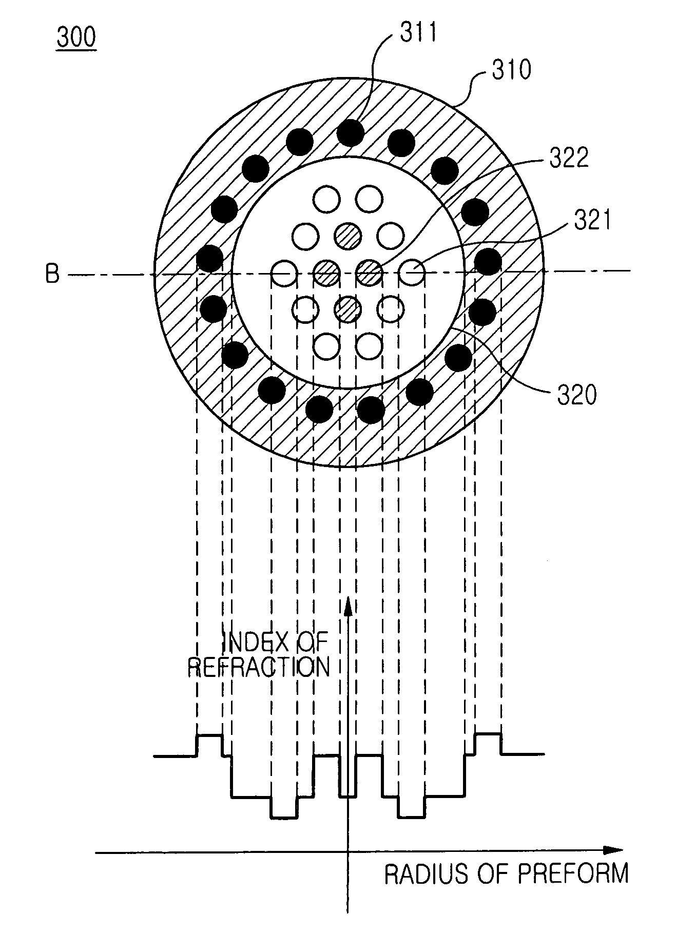
[0029]FIG. 3 depicts, by way of illustrative and non-limitative example, in cross section a photonic crystal fiber preform 100 according to a first preferred embodiment of the present invention.

[0030]The photonic crystal fiber preform 100 is made up of a rod-shaped substrate 110 with a plurality of holes longitudinally formed therethrough in a photonic lattice structure. Each of the holes has a circular cross section, and the diameter of each of the holes is smaller than that of the rod-shaped substrate 110. The holes are uniformly spaced apart from each other to form a hexagonal pattern, and are filled with materials having at least two different indices of refraction 120, 130, 140, respectively. Distribution of index of refraction of the photonic cr...


PUM

PropertyMeasurementUnit
dielectric constantaaaaaaaaaa
photonic lattice structureaaaaaaaaaa
indices of refractionaaaaaaaaaa

Abstract

A photonic crystal fiber (PCF) preform, from which a photonic crystal fiber is manufactured, includes a rod-shaped substrate with holes longitudinally formed therethrough in a photonic lattice structure, and material layers having at least two different indices of refraction. The material layers are disposed in the holes, respectively. Distribution of index of refraction of the photonic crystal fiber preform is controlled by arrangement of the material layers. Consequently, an optical fiber with very low optical loss, very low optical nonlinearity and excellent transmission characteristics can be easily manufactured, and an optical fiber with various characteristics, differing depending upon the lattice structure, can be realized.

Description

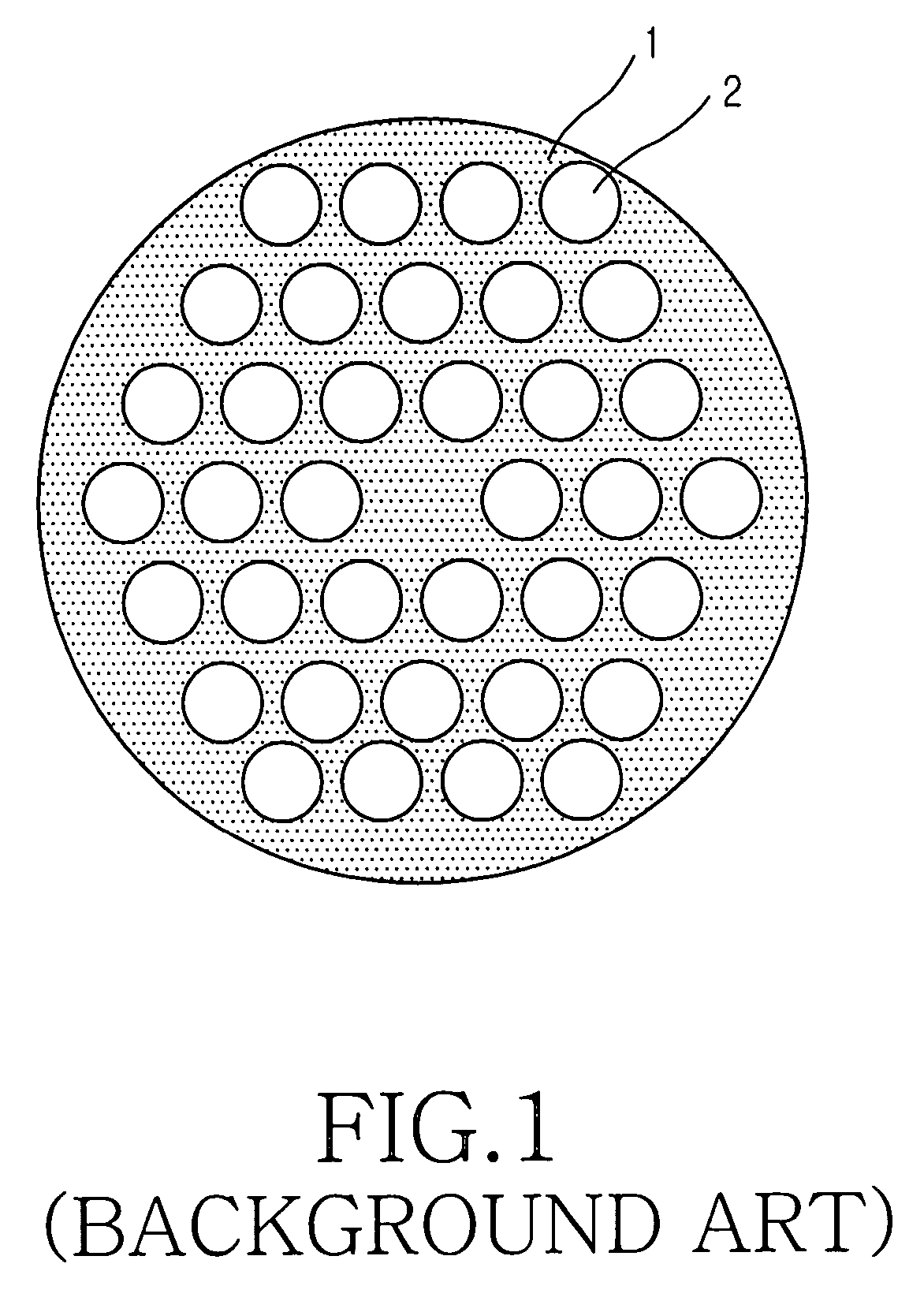
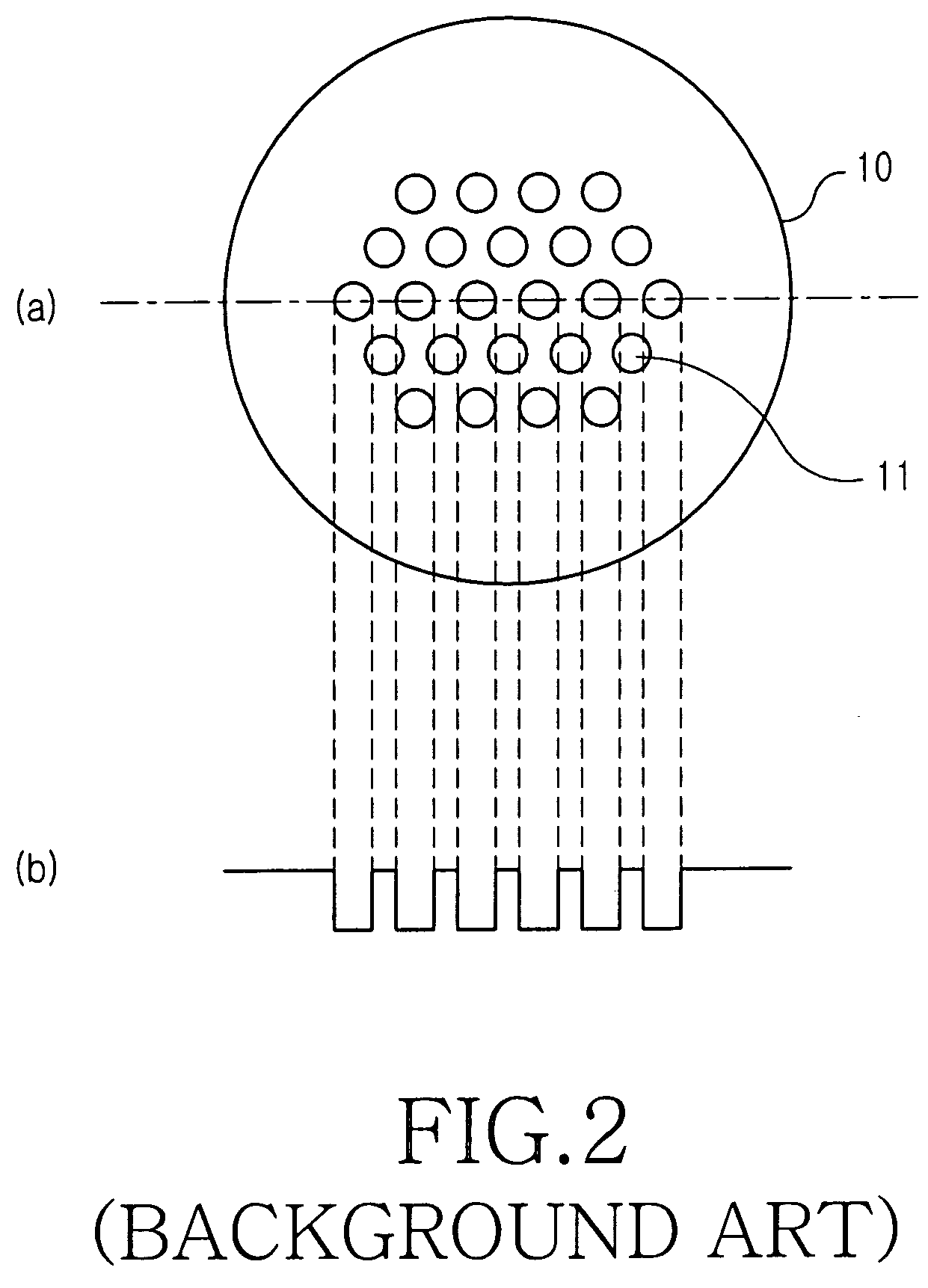
CLAIM OF PRIORITY[0001]This application claims priority to an application entitled “PHOTONIC CRYSTAL FIBER PREFORM AND PHOTONIC CRYSTAL FIBER MANUFACTURED USING THE SAME,” filed in the Korean Intellectual Property Office on May 29, 2003 and assigned Ser. No. 2003-34387, the contents of which are hereby incorporated by reference.BACKGROUND OF THE INVENTION[0002]1. Field of the Invention[0003]The present invention relates to a photonic crystal fiber (PCF) preform and a photonic crystal fiber manufactured using the same.[0004]2. Description of the Related Art[0005]A photonic crystal fiber (PCF) is a special kind of optic fiber. A general single-mode optical fiber is made up of a core material which consists of glass and germanium or phosphorus. On the other hand, the photonic crystal fiber is made up of a single, solid and substantially transparent material 1, such as silica glass, and periodically spaced air holes 2 running along the fiber, as shown in FIG. 1. Difference in dielectric...

Claims


Application Information

Patent Timeline
Patent Type & Authority Patents(United States)
IPC IPC(8): G02B6/02G02B6/00G02B6/032C03B37/012
CPCC03B37/0122G02B6/02357G02B6/02366G02B6/0238C03B2203/42G02B6/028G02B6/00
Inventor OH, SUNG-KOOGLEE, JAE-HO
Owner SAMSUNG ELECTRONICS CO LTD
Learn More