
Preventing plasma induced damage resulting from high density plasma deposition

a plasma deposition and high density technology, applied in the field of plasma induced damage, can solve problems such as device failure, thin gate oxide layer damage, device failure, etc., and achieve the effects of preventing device failure, preventing plasma induced damage, and preventing device failur

Inactive Publication Date: 2007-04-24
CHARTERED SEMICONDUCTOR MANUFACTURING
View PDF22 Cites 12 Cited by
  • Summary
  • Abstract
  • Description
  • Claims
  • Application Information

AI Technical Summary

Benefits of technology

[0009]The present invention provides a method and apparatus for preventing plasma induced damage resulting from high density plasma deposition processes. More particularly, the method and apparatus of the present invention prevents plasma-induced damage to ultra-thin gate oxide of underlying semiconductor devices. In addition, the method and apparatus of the present invention is suitable for sub 0.18 micron fabrication processes and does not reduce the gap-fill capability of the high density plasma deposition process.
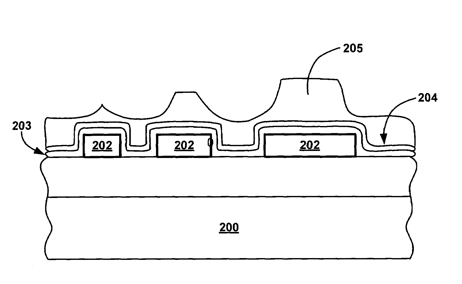
[0012]A silicon-rich oxide is then deposited to form a silicon-rich oxide liner. In the present embodiment, the silicon-rich oxide liner is deposited in-situ immediately following deposition of the USG liner such that the silicon-rich oxide liner directly overlies the USG liner. The silicon-rich oxide liner protects the metal structure from plasma charge during the subsequent high density plasma deposition process.
[0013]The high density plasma deposition process can then be performed. During the high density plasma deposition process, the underlying silicon-rich oxide liner prevents damage to underlying structures. More particularly, because silicon-rich oxide has lower high density plasma removal rate than a conventional USG liner, the use of a silicon-rich oxide liner is more effective than conventional USG liners in preventing damage during high density plasma deposition processes. In addition, because the silicon-rich liner is more dense than a conventional USG liner, a thin silicon-rich liner is sufficient to protect the underlying metal structures from corner clipping; thereby preventing metal structures from being exposed to plasma charge. By preventing exposure of metal structures to plasma charge, damage to the ultra-thin oxide layer of underlying devices is avoided.
[0014]The thin silicon-rich liner of the present invention does not significantly reduce the gap-fill capability of the high density plasma deposition process. Thereby, a structure with good fill characteristics is obtained.
[0016]The method and apparatus of the present invention is suitable for sub 0.18 micron fabrication processes. Thus, as geometry's continue to shrink in size, the method and apparatus of the present invention effectively allows for production of CMOS devices, preventing device failures associated with plasma-induced damage resulting from high density plasma deposition processes.
[0017]The present invention provides a method and apparatus for preventing plasma induced damage resulting from high density plasma deposition processes. In addition, the present invention provides a method and apparatus for preventing plasma induced damage to the ultra-thin gate oxide of underlying devices. In addition, the present invention provides a method and apparatus that is suitable for sub 0.18 micron fabrication processes. Moreover, the present invention provides a method and apparatus that does not reduce the gap-fill capability of the high density plasma deposition process.

Problems solved by technology

However, one problem that arises in the fabrication of sub 0.18 micron semiconductor devices is that high density plasma deposition processes can damage the underlying ultra-thin gate oxide layer, leading to device failures.
More particularly, when a high density plasma deposition process is performed over a metal interconnect structure, plasma charge is conveyed through the metal interconnect structure to the underlying devices, damaging the thin gate oxide layer and resulting in device failure.
However, deposition with low deposition-to-sputter ratio can generate non-uniform plasma and can cause radiation damage to underlying semiconductor devices.
However, it is difficult to optimize the thickness of the pre-deposited liner.
A thin liner is not sufficient to protect the underlying gate oxide from high density plasma related damage.
A thick liner is effective for preventing charging damage, but strongly reduces the gap-fill capability of the high density plasma deposition process.
Therefore, it is difficult to obtain a USG liner that is effective for protecting the metal interconnect from plasma charge and that does not significantly reduce the gap-fill capabilities of the high density plasma deposition process.
Thus, plasma related damage often occurs in spite of the use of a USG liner(e.g., as a result of nonuniformities in the USG liner or as a result of corner clipping).

Method used


Image

  • Preventing plasma induced damage resulting from high density plasma deposition
  • Preventing plasma induced damage resulting from high density plasma deposition
  • Preventing plasma induced damage resulting from high density plasma deposition

Examples


Embodiment Construction

[0024]In the following detailed description of the present invention, numerous specific details are set forth in order to provide a thorough understanding of the present invention. However, it will be recognized by one skilled in the art that the present invention may be practiced without these specific details or with equivalents thereof. In other instances, well known methods, procedures, components, and circuits have not been described in detail as not to unnecessarily obscure aspects of the present invention.

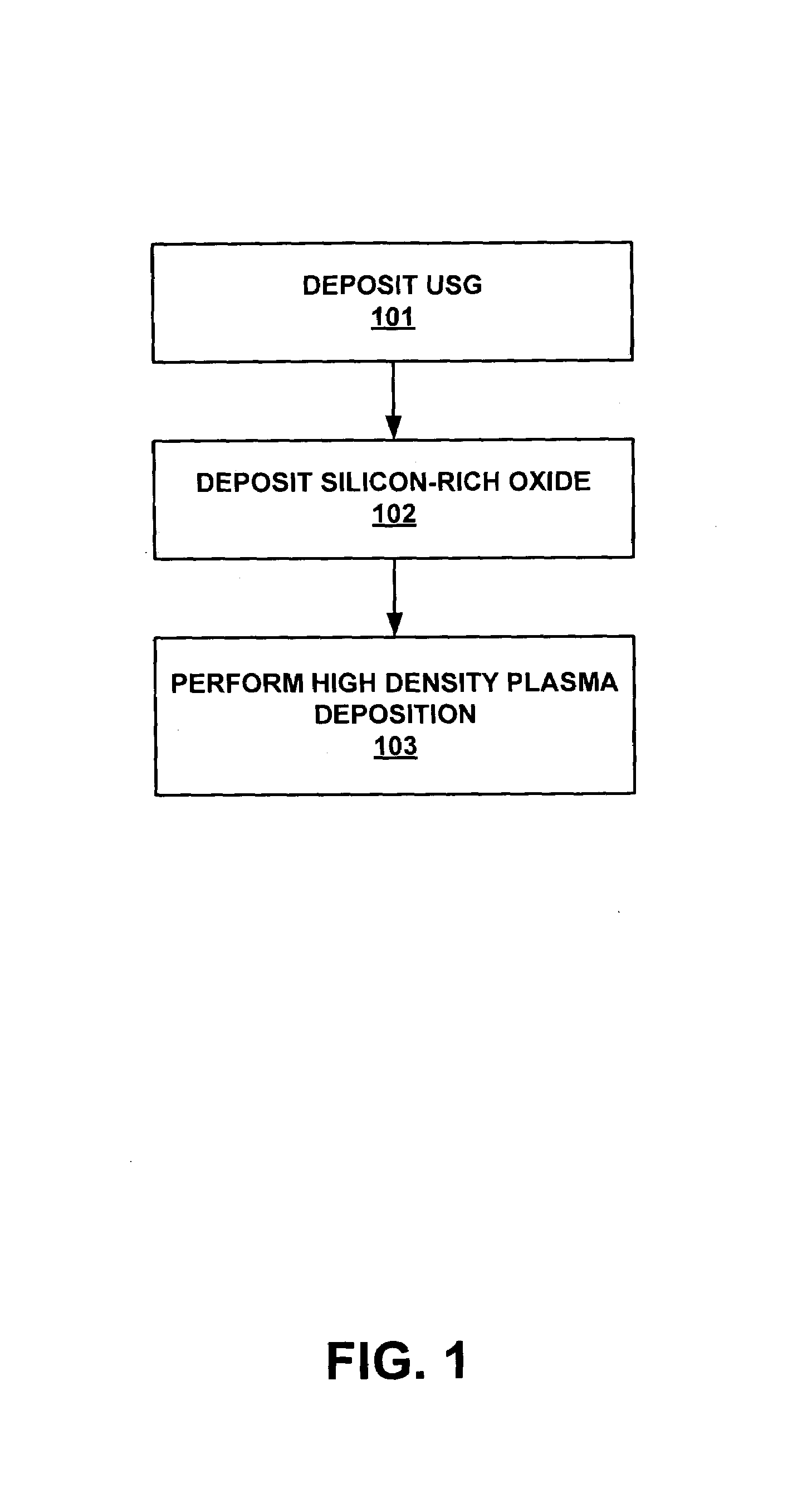
[0025]FIG. 1 shows a method for preventing plasma induced damage resulting from high density plasma deposition processes in accordance with one embodiment of the present invention. First, as shown by step 101, Un-doped Silica Glass(USG) is deposited. In the present embodiment, USG is deposited in-situ so as to form a USG liner.

[0026]Continuing with step 101, in the present embodiment, USG is deposited so as to form a USG liner having a thickness of from 50 to 200 Angstroms. ...


PUM


Abstract

A method and apparatus for preventing plasma induced damage resulting from high density plasma deposition processes. In the present embodiment, Un-doped Silica Glass(USG) is deposited so as to form a USG liner. In the present embodiment, the USG liner directly overlies a conductive interconnect structure that couples to semiconductor devices that are susceptible to plasma-induced damage during high density plasma deposition processes. A silicon-rich oxide is deposited in-situ immediately following the deposition of the USG liner so as to form a silicon-rich oxide liner that directly overlies the USG liner. The silicon-rich oxide liner protects the interconnect structure during the subsequent high density plasma deposition process, preventing damage resulting from plasma charge to the interconnect structure.

Description

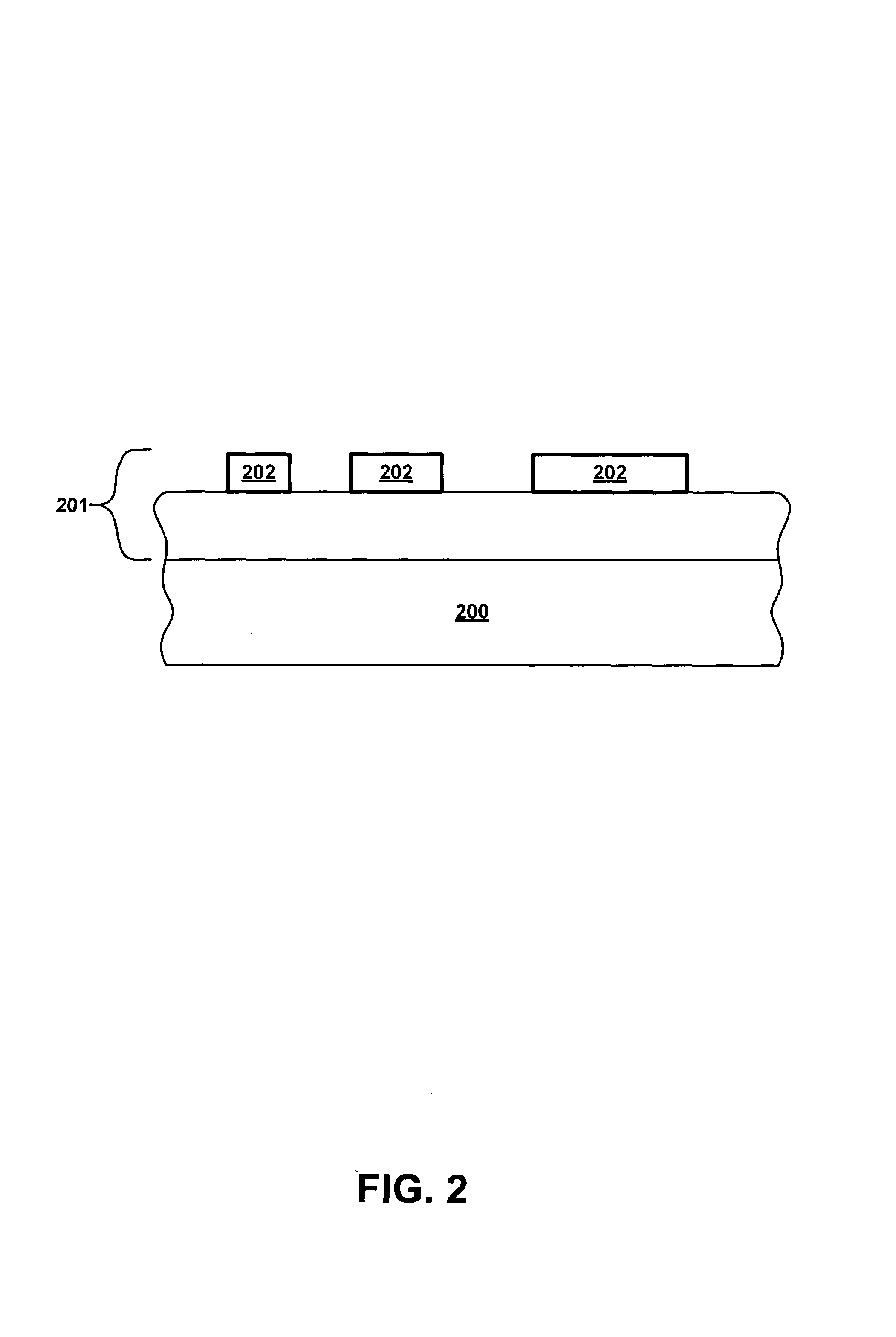
BACKGROUND OF THE INVENTION[0001]1. Field of the Invention[0002]The present invention relates to the field of semiconductor devices. More particularly, the present invention relates to a method and apparatus for preventing plasma induced damage that results from high density plasma deposition processes.[0003]2. Related Art[0004]In conventional in Complimentary Metal Oxide Semiconductor (CMOS) device fabrication processes, semiconductor devices are formed on a semiconductor substrate using a thin gate oxide layer that forms gates between conductive regions in the semiconductor substrate. Overlying metal interconnect structures provide for electrical connection to the underlying semiconductor devices.[0005]As semiconductor devices continue to be reduced in size, fabrication process have evolved that use ultra-thin gate oxide layers. These ultra-thin gate oxide layers are desirable for forming semiconductor devices having sizes smaller than 0.18 microns. However, one problem that arise...

Claims


Application Information

Patent Timeline
IPC IPC(8): H01L21/31H01L23/58H01L21/316H01L21/768
CPCH01L21/02164H01L21/02274H01L21/02304H01L21/31612H01L21/76832H01L21/76834H01L21/02131H01L21/02211
Inventor HUANG, LIUSODIJONO, JOHN
Owner CHARTERED SEMICONDUCTOR MANUFACTURING
Learn More