Heating element CVD system and connection structure between heating element and electric power supply mechanism in the heating element CVD system

Inactive Publication Date: 2007-05-01
CANON ANELVA CORP
11 Cites 9 Cited by

AI-Extracted Technical Summary

Problems solved by technology

Further, in the heating element CVD method, plasma is not produced, as it is produced in the plasma CVD method.
As a result, the heating power is reduced and the whole heating element is finally deteriorated.
Also, it reduces a film forming speed as hours of use of the heating element is elongated.
Further, since the products of the silicide and the like have high vapor pressures in general, they contaminate the deposited film and degrade the quality of the silicon film formed or the silicon nitride film formed as the deterio...

Benefits of technology

[0052]Thus, even if a case where the sealing member, such as the O ring, is used in the connection terminal holder, the temperature of the connection terminal holder can be prevented from exceeding the heat resistance temperature of the sealing member, so that it is possible to improve the stability of the heating element CVD system. Further, if the connection terminal holder is cooled by the cooling mechanism in order to prevent the temperature of the connection terminal holder from exceeding the heat resistance temperature of the sealing member, the film is deposited on the surface of the shield plate...

Abstract

A heating element CVD system wherein one or a plurality of connection terminal holders is placed in the processing container, and each of the connection terminal holders holds a plurality of connection terminals. Each of the connection terminals connects the heating element to the electric power supply mechanism electrically such that a connection region of the heating element connected to the connection terminal is not exposed to a space in the processing container.

Application Domain

Muffle furnacesHeater elements +7

Technology Topic

ElectricityEngineering +3

Image

  • Heating element CVD system and connection structure between heating element and electric power supply mechanism in the heating element CVD system
  • Heating element CVD system and connection structure between heating element and electric power supply mechanism in the heating element CVD system
  • Heating element CVD system and connection structure between heating element and electric power supply mechanism in the heating element CVD system

Examples

  • Experimental program(1)

Example

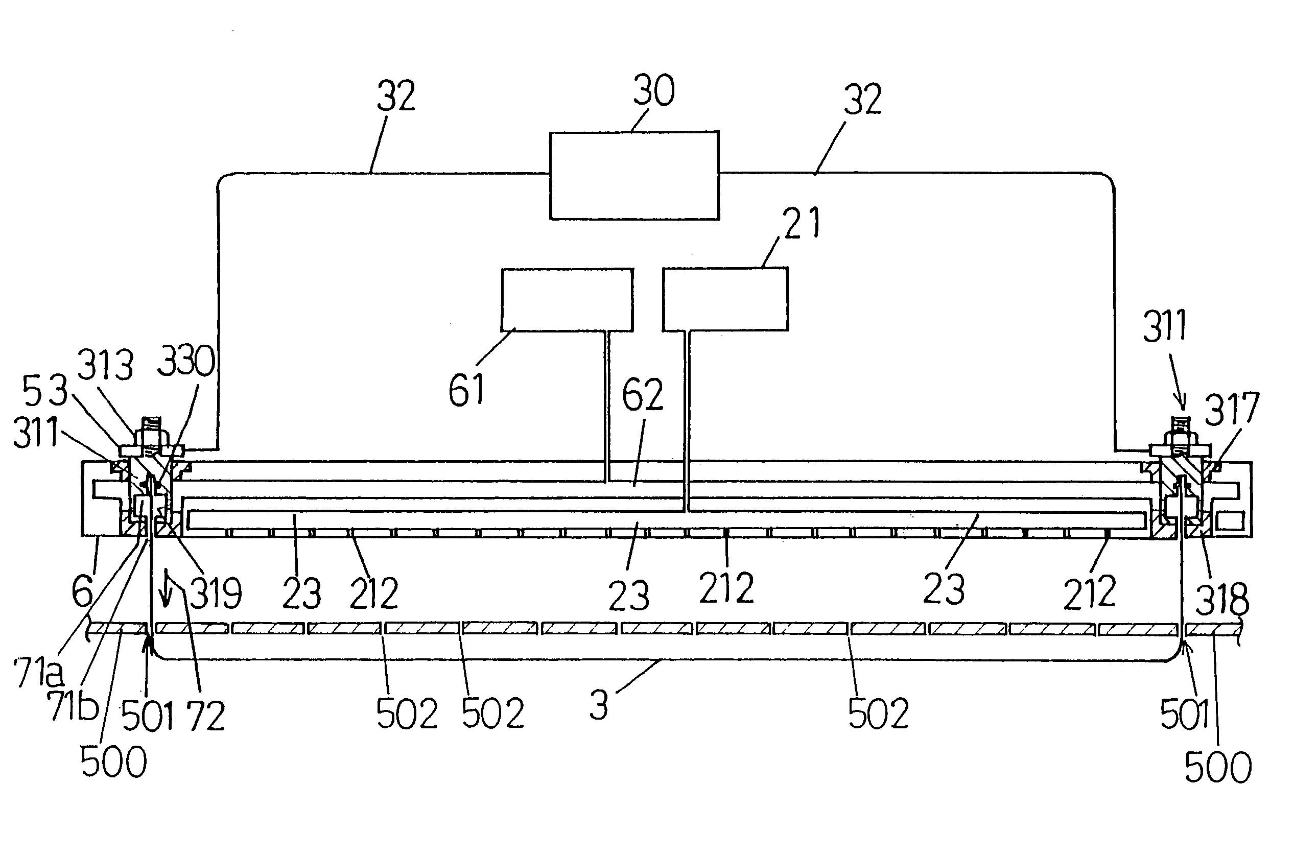
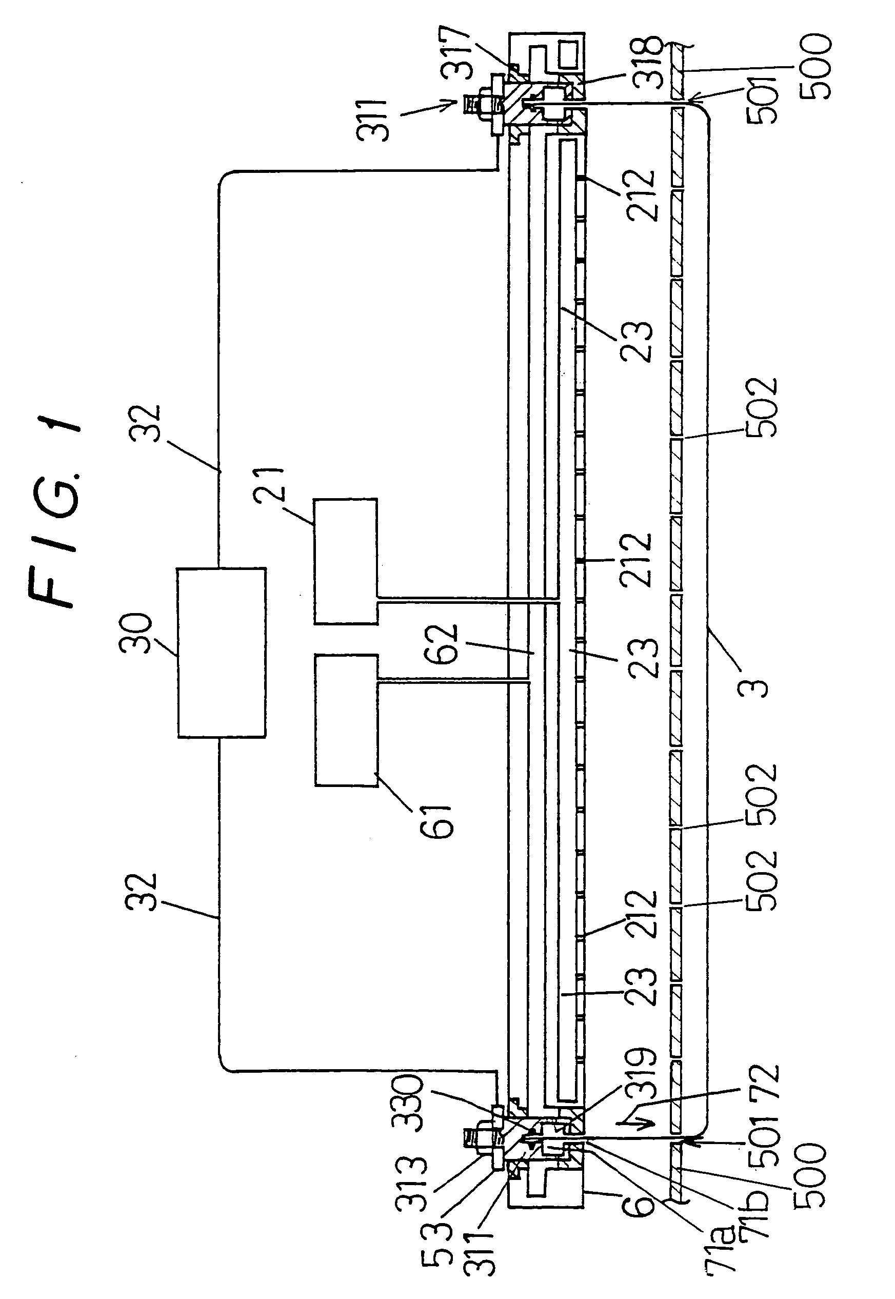
[0062]Preferred embodiments of the present invention will hereinafter be described on the basis of the accompanying drawings.
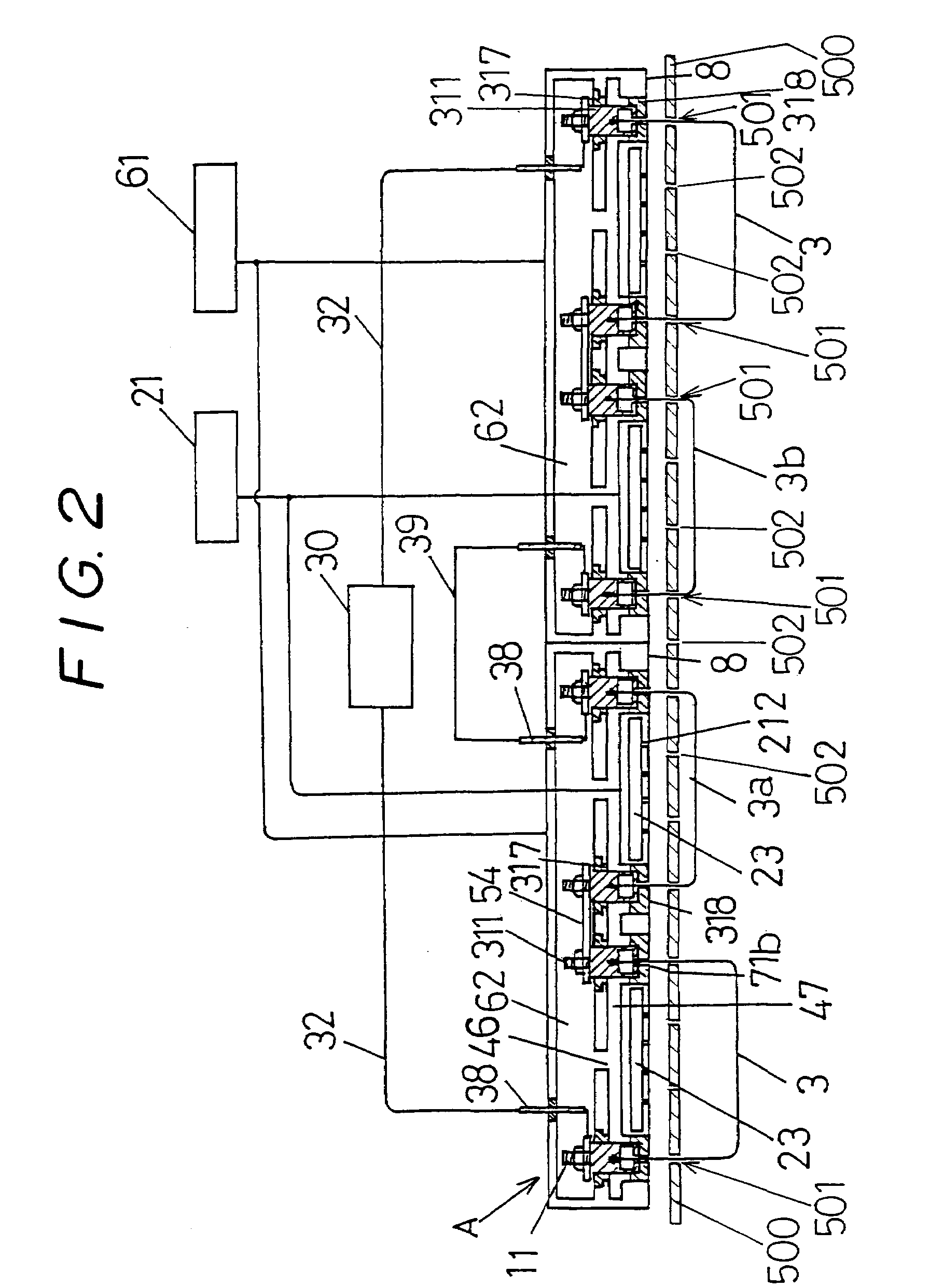
[0063]FIGS. 1 and 2 show a cross-sectional structure of a connection part between a heating element and an electric power supply mechanism in a preferred embodiment of a heating element CVD system in accordance with the invention.
[0064]The structures of a processing container 1, a substrate holder 4, and an evacuation system 11 and the like in a heating element CVD system in accordance with the invention are the same as those of the above-mentioned conventional heating element CVD system shown in FIG. 7, and hence are omitted in the drawings. Further, same reference numerals are attached to members similar to the members shown in FIG. 7.
[0065]In the embodiment shown in FIG. 1, a connection terminal 311 is held by a connection terminal holder 6 having a first inside hollow portion 62 therein with electrical insulation by insulators 317 and 318.
[0066]In the embodiment shown in FIG. 2, a connection terminal 311 is held by a connection terminal holder 8 having a first inside space 62 therein with electrical insulation by insulators 317 and 318.
[0067]In the embodiment shown in FIG. 1, a power supply line 32 from the electric power supply mechanism 30 is connected to a power supply plate 53. The power supply plate 53 is sandwiched between a nut 313 and the connection terminal 311. On the other hand, the end portion of a heating element 3 is pressed onto and connected to the connection terminal 311 by a coil spring 330.
[0068]In this manner, the end portion of the power supply line 32 from the electric power supply mechanism 30 is connected to the end portion of the heating element 3 via the connection terminal 311.
[0069]Each of the connection terminal holders 6 (FIG. 1) and 8 (FIG. 2) supports the heating element 3 such that the heating element 3 faces a substrate holder 4. And each of the connection terminal holders 6 and 8 is a structural body independent of a processing container 1. Also, each of these connection terminal holders 6, 8 is connected to the electric power supply mechanism 30, a raw material gas supply system 21 and a gas introduction system 61.
[0070]The connection terminal 311 has a connection terminal inside hollow portion 71a at the side toward the inside of the processing container 1 (lower side in FIGS. 1 and 2) and has a gas passing hole 71b, through which the connection terminal inside hollow portion 71a communicates with the inside of the processing container 1, in a part facing the processing container 1.
[0071]The heating element 3 is connected to the connection terminal 311 through these gas passing holes 71b and the connection terminals inside hollow portion 71a in a state where it is not put into contact with the connection terminal 311 at the part of the gas passing hole 71b and the connection terminal inside hollow portion 71a.
[0072]As described above, in this structure, the connection region of the heating element 3 connected to the connection terminal 311 is not exposed to a space in the processing container 1. With this structure, when the film is formed, it is possible to prevent a raw material gas such as a silane gas or the like from contacting the connection region of the heating element 3 connected to the connection terminal 311 (a part of heating element 3 where its temperature is slightly low), and when a deposited film is removed (a cleaning operation is performed), it is possible to prevent a cleaning gas from contacting the connection region of the heating element 3 connected to the connection terminal 311 (a part of heating element 3 where its temperature is slightly low).
[0073]Gas can be passed, by a gas passage 319, between the connection terminal inside hollow portion 71a and the first inside hollow portion 62 in the connection terminal holder 6. Further, there is provided a gas introduction system 61 for introducing gas into the first inside hollow portion 62 in the connection terminal holder 6.
[0074]In the embodiment shown in FIG. 1, the gas passage 319 is drawn at the side of the connection terminal 311 where the heating element 3 is connected, but it is possible to face the gas passage 319 to the part where the heating element 3 is just connected to the connection terminal 311.
[0075]The gas introduction system 61 is a gas introduction system for introducing any one gas of hydrogen, argon, helium, neon, krypton, xenon, nitrogen, or ammonia, or a mixed gas containing two or more kinds of these gases. This gas supply system 61 has the same constitution as the raw material gas introduction system 21 shown in FIG. 7.
[0076]In the embodiment shown in FIG. 1, as described above, the gas (purge gas) introduced by the gas introduction system 61 is introduced into the processing container 1 through the first inside hollow portion 62, the gas passage 319, the connection terminal inside hollow portion 71a and the gas passing hole 71b.
[0077]Accordingly, when the film is formed, it is possible to further effectively prevent the raw material gas such as a silane gas or the like from contacting the connection region of the heating element 3 connected to the connection terminal 311 (the part of the heating element 3 where its temperature is slightly low). Further, when the deposited film is removed (the cleaning operation is performed), it is possible to further prevent the cleaning gas from contacting the connection region of the heating element 3 connected to the connection terminal 311 (the part of the heating element 3 where its temperature is slightly low).
[0078]Further, in the embodiments shown in FIGS. 1 and 2, each of the connection terminal holders 6 and 8 has a second inside hollow portion 23. A raw material gas supply system 21 is connected to this second inside hollow portion 23. Also, the second inside hollow portion 23 has a plurality of gas blowing-out openings 212 made in the surface on the side facing the substrate holder 4. The second inside hollow portion 23 communicates with the space in the processing container 1 only through the gas blowing-out openings 212. That is, as shown in FIGS. 1 and 2, the first inside hollow portion 62 is separated from the second inside hollow portion 23.
[0079]In this connection, while only one heating element 3 is shown in the embodiment shown in FIG. 1, the number of the heating elements 3 is arbitrarily selected and, needless to say, the connection terminal holder 6 is provided with the connection terminals 311 of the number corresponding to the number of the heating elements 3.
[0080]In the embodiment shown in FIG. 1, the raw material gas is supplied into the processing container 1 through the gas blowing-out openings 212 from the second inside hollow portion 23. Therefore, even if a substrate to be processed has a large area, by enlarging the connection terminal holder 6 and increasing the number of the heating elements 3, the raw material gas can be supplied to the whole surface of the large-area substrate, whereby a uniform film can be formed. That is, this embodiment can easily be applied to a substrate having a large area.
[0081]The hydrogen gas can be introduced, as shown by an arrow 72, into the processing container 1 from the gas supply system 61 through the first inside hollow portion 62 of the connection terminal holder 6, the gas passage 319, the connection terminal inside hollow portion 71a, and the gas passing hole 71b.
[0082]This flow of the hydrogen gas can prevent the silane gas, introduced into the processing container 1 from the raw material gas supply unit 21, and/or the activated species originated from the silane gas, which are decomposed and/or activated on the surface of the heating element 3, from entering into the connection terminal inside hollow portion 71a through the gas passing hole 71b. This can prevent the silane gas and/or the activated species originated from the silane gas from contacting the connection terminal 311 of the heating element 3, thereby preventing a part of the heating element 3, where its temperature is slightly low, from being changed to a silicide and degraded.
[0083]In the above-mentioned embodiment in accordance with the invention, when a film deposited on the inside of the processing container 1 is removed (cleaned), the respective gases are introduced as follows.
[0084]In the case of the embodiment shown in FIG. 1, the cleaning gas is introduced into the processing container 1 from a cleaning gas supply system (not shown), the construction of which is similar to the raw material gas supply system 21, through the second inside hollow portion 23 and the gas lowing-out openings 212, and any one gas of hydrogen, argon, helium, neon, krypton, xenon, nitrogen, or ammonia, or a mixed gas of two or more kinds of these gases is introduced, as shown by the arrow 72, into the processing container 1 from the gas supply system 61 through the first inside hollow portion 62 of the connection terminal holder 6, the gas passage 319, the connection terminal inside hollow portion 71a, and the gas passing hole 71b.
[0085]This can prevent the cleaning gas itself and/or the activated species originated from the cleaning gas, which are decomposed and/or activated on the surface of the heating element 3, from entering into the connection terminal inside hollow portion 71a. Thus, it is possible to prevent the part of the heating element 3 where its temperature is slightly low (the connection region of the heating element 3 connected to the connection terminal 311) from being etched and degraded.
[0086]Each of FIGS. 2 and 3 shows a cross sectional structure of the connection part between the heating element and the electric power supply mechanism in another embodiment in which a plurality of connection terminal holders 6, described in FIG. 1, are provided in the processing container 1.
[0087]The part shown in this FIG. 2 corresponds to the part shown in FIG. 1. FIG. 3(a) shows in detail the part A indicated in FIG. 2. As is the case with FIG. 1, the structures of the processing container 1, the substrate holder 4, the evacuation system and the like are the same as those of the conventional heating element CVD system shown in FIGS. 7 and 8. Therefore, their illustrations and descriptions will be omitted.
[0088]In the embodiment shown in FIG. 2, a nut 313 fixes the connection terminal 311 to the connection terminal holder 8 and, at the same time, connects the connection terminal 311 to the power supply plates 53, 54.
[0089]The basic structure and construction in the embodiment shown in FIG. 2 is the same as those in the embodiment shown in FIG. 1. Therefore, in FIG. 2, the same reference numerals are attached to the members similar to members shown in FIG. 1 and their descriptions will be omitted.
[0090]In the embodiments shown in FIGS. 1 to 3, the heating element 3 is connected to and held by the connection terminal 311 by a coil spring 330. With this coil spring 330, the heating element 3 can be mounted on or dismounted from the connection terminal 311 with a single motion.
[0091]The embodiment shown in FIG. 2 is different from the embodiment shown in FIG. 1 in that two connection terminal holders 8 are disposed in the processing container 1 and that the connection part connecting the connection terminal and the electric power supply mechanism and the wiring part for electrically connecting the connection terminals are built in the connection terminal holder 8. Then, the difference in the structure between the embodiment shown in FIG. 2 and the embodiment shown in FIG. 1 will specifically be described in the following.
[0092]In the embodiment shown in FIGS. 2 and 3, the connection part connecting the connection terminal 311 and the electric power supply mechanism 30 is covered with the first inside hollow portion 62. This can prevent the connection part connecting the connection terminal 311 and the electric power supply mechanism 30 from being exposed to the space in the processing container 1. Further, also the power supply plate 54 (between the connection terminals) that is the wiring portion for electrically connecting the connection terminals is covered with the first inside hollow portion 62. Thereby, the power supply plate 54 can be prevented from being exposed to the space in the processing container 1.
[0093]In the embodiment shown in FIGS. 2 and 3, the connection terminal 311 is provided with a gas passage 319 for connecting an inside hollow portion 47 in the connection terminal holder 8 to the connection terminal inside hollow portion 71a. Thus, the gas introduced from the gas introduction system 61 fills the first inside hollow portion 62 and is introduced into the next inside hollow portion 47 through an inside hollow portion penetrating hole 46. The gas is further flowed into the connection terminal inside hollow portion 71a in the connection terminal 311 through the gas passage 319. Then, the gas passes near the heating element 3 and the coil spring 330 to the non-contact part between the heating element 3 connected to the connection terminal 311 and the connection terminal holder 8. That is, the gas flows to the space in the processing container 1 through the gas passing hole 71b, as shown by the arrow 72.
[0094]The heating element CVD system shown in FIGS. 1 and 2, is characterized in that a shield plate 500 is arranged on a side (bottom side in FIGS. 1 and 2) facing the inside of the processing container 1, that is, 6 (FIG. 1) and 8 (FIG. 2) respectively.
[0095]The shield plate 500 has heating element passing holes 501 and a plurality of through holes 502. The heating element 3 can pass through the heating element passing holes 501 in a noncontact manner. And the gas can pass through the through holes 502.
[0096]As shown in FIGS. 1 and 2, the heating element 3 extends through the heating element passing holes 501 into the processing container 1, so that the shield plate 500 is arranged between the part of the heating element 3 extending into the processing container 1 through the heating element passing holes 501 and a surface of the connection terminal holder 6 or 8 facing the inside of the processing container 1.
[0097]In the heating element CVD system, a sealing member (not shown) such as an O ring needs to be used, for example, in order to completely separate the first inside hollow portion 62 from the second inside hollow portion 23 in the connection terminal holder 6 or 8 and to completely separate these hollow portions 62 and 23 from the space in the processing container 1, or in a case where a structural body such as the connection terminal 311 is arranged in the inside hollow portion 47 of the connection terminal holder 8.
[0098]However, since the connection terminal holder 6 or 8 is heated by the radiant heat of the heating element 3, in some cases, its temperature far exceeds the heat resistance temperature of the sealing member such as the O ring (150° C. for Viton and 280° C. for top-rated Kalrez). In this case, the connection terminal holder 6 or 8 needs to be cooled to a temperature lower than the heat resistance temperature of the sealing member such as the O ring, for example, by a cooling mechanism (not shown).
[0099]On the other hand, in a case where a Si film is formed by using SiH4 or SiH4+H2 as a raw material gas in a Cat-CVD system, H radicals have a significant effect on the film characteristics. Thus, when the connection terminal holder 6 or 8 is cooled to the temperature lower than the heat resistance temperature of the sealing member such as the O ring, as described above, the H radicals produced when the raw material gas is put into contact with and decomposed by the heating element 3 react with the film deposited on the surface of the connection terminal holder 6 or 8. As a result, there is a possibility that the amount of H radicals in the processing container 1 might decrease to degrade the film characteristics. Further, there is also a possibility that a substance produced by the before described reaction of the H radicals with the film deposited on the surface of the connection terminal holder 6 or 8 as well as the other substance produced by decomposition and activation of the before described substance by the heating element 3 are also taken into the film formed on the substrate placed on the substrate holder 4, thereby the film characteristics is degraded.
[0100]According to the heating element CVD system shown in FIGS. 1, 2 and 3(a), the shield plate 500 is arranged between the part of the heating element 3 extending into the processing container 1 through the heating element passing hole 501 of the shield plate 500 and the surface of the connection terminal holder 6 or 8 facing the inside of the processing container 1, so that the connection terminal holder 6 or 8 is not heated by the radiant heat of the heating element 3.
[0101]As a result, although any cooling mechanism is not used, it is possible to prevent the temperature of the connection terminal holder 6 or 8 from exceeding the heat resistance temperature of the sealing member such as the O ring.
[0102]In addition, the film is deposited on the surface of the shield plate 500 facing the inside of the processing container 1 and heated by the radiant heat of the heating element 3. And at this time, the shield plate 500 is heated, thus, the deposited film does not react with the H radicals, and hence the amount of H radicals in the space in the processing container 1 does not decrease, which can prevent the deterioration of the film characteristics.
[0103]It is possible to connect the shield plate 500 to a temperature adjusting mechanism (not shown) and to keep the shield plate 500 at a predetermined temperature (250° C. to 500° C.).
[0104]Next, a connection structure between the heating element 3 and the electric power supply mechanism 30 that is distinctive in the heating element CVD system of an embodiment of the invention will be described.
[0105]As shown in FIG. 3(a), a connection pin 503 is provided on the end of the heating element 3. On the other hand, the connection terminal 311 has a pin receiver 504 having a small hole 505 through which the connection pin 503 is inserted or removed. The inside diameter of the small hole 505, as shown in FIG. 3(c), is smaller than the diameter of the connection pin 503. As shown in FIGS. 3(b) and 3(c), the peripheral wall of the pin receiver 504 forming the small hole 505 is provided with slits 506 extending laterally to the direction in which the connection pin 503 is inserted or removed. In this connection, FIG. 3(b) illustrates the pin receiver 504 when it is viewed from the direction in which the connection pin 503 is inserted or removed (from the bottom side in FIGS. 3(a) and FIG. 3(c) is a side view showing the state where the connection pin 503 is inserted into the pin receiver 504, parts being partially omitted for clearness.
[0106]A wire-shaped material having a diameter of about 0.5 mm is usually used as the heating element 3. Thus, since the heating element 3 is connected to the connection terminal 311 by the connection structure in which the connection pin 503 is provided on the end of the heating element 3 and is inserted into or removed from the small hole 505 of the pin receiver 504 provided on the connection terminal 311, the diameter of the connection part can be enlarged as compared with a case where the end of the heating element 3 provided with no connection pin 503 is connected to the connection terminal 311, whereby an electric contact area can be enlarged.
[0107]In a case where the end of the heating element 3, usually having a small diameter, is connected to the connection terminal 311, the contact area is small, so that the end of the heating element 3 is heated by contact resistance. Thus, there is a possibility that the spring ability of the coil spring 330 for keeping the electric contact with the heating element 3 and holding the heating element 3 might be degraded by the heat generated.
[0108]However, in the present invention, by connecting the heating element 3 to the connection terminal 311 via the connection pin 503 provided on the end of the heating element 3, as described above, it is possible to enlarge the electric contact area and hence to reduce contact resistance and thus to prevent heat from being generated by the contact resistance.
[0109]Further, the inside diameter of the small hole 505, which is made in the pin receiver 504 of the connection terminal 311 in which the connection pin 503 provided on the end of the heating element 3 is inserted, is smaller than the diameter of the connection pin 503, and the slits 506 extending laterally to the direction in which the connection pin 503 is inserted or removed are formed in the peripheral wall of the pin receiver 504 forming the small hole 505. Thus, the pin receiver 504 is formed as a pin receiver having a spring ability.
[0110]Then, when the connection pin 503 is inserted in the small hole 505 of the pin receiver 504 from the direction shown by an arrow in FIG. 3(c), a good thermal contact between the connection terminal 311 and the connection pin 503 can be achieved by the above-mentioned spring ability to dissipate heat from the heating element 3 heated by passing electric current to the connection terminal 311 to thereby prevent the connection pin 503 from being heated. This can more effectively prevent the possibility that the spring ability of the coil spring 330 for keeping the electric contact with the heating element 3 and holding the heating element 3 from being degraded.
[0111]Also, a good thermal contact as well as a better electric connection can be achieved by inserting the connection pin 503 provided on the end of the heating element 3 into the small hole 505 of the pin receiver 504 having the above-mentioned spring ability, thereby it can further reduce the contact resistance and prevent excessive heating caused by the contact resistance.
[0112]FIGS. 5(a) and 5(b) illustrates another connection structure between the heating element 3 and the electric power supply mechanism 30.
[0113]In a case where the heating element 3 is supported by the coil spring 330, if a thermal expansion in the direction indicated by a reference symbol 507 in FIG. 4 of the heating element 3 becomes large, there is a possibility that the heating element 3 will contact an insulator 318 at the gas passing hole 71b. Such contact reduces the temperature of the heating element 3 at the contacted part and hence causes a problem of silicide formation in case of forming the film and a problem of etching in case of cleaning.
[0114]In the connection structure between the heating element 3 and the electric power supply mechanism 30 shown in FIGS. 5(a) and 5(b), in addition to the connection structure described by the use of FIGS. 3(a) to 3(c), a spacer 508 is provided. This spacer 508 is arranged between the inner peripheral wall of the heating element passing hole 509 and the connection pin 503 on the opening side facing the connection terminal inside hollow portion 71a of the heating element passing hole 509 connecting the connection terminal inside hollow portion 71a and the pin receiver 504.
[0115]According to this structure, the heating element 3 is fixed at least at two positions of the pin receiver 504 and the spacer 508, so that the inclination a of the heating element 3 caused by thermal expansion in the direction indicated by the arrow 507 can be reduced. Thus, even in a case where the elongation caused by the thermal expansion in the direction indicated by the arrow 507 in FIG. 4 of the heating element 3 is enlarged, it is possible to exclude the possibility that the heating element 3 might be put into contact with the insulator 318 at the gas passing hole 71b.
[0116]FIG. 6 shows still another connection structure of the heating element 3 and the electric power supply mechanism 30.
[0117]In the embodiment shown in FIG. 2, the connecting part between the connection terminal 311 and the electric power supply mechanism 30 is covered with the first inside hollow portion 62. This structure prevents the connecting part between the connection terminal 311 and the electric power supply mechanism 30 from being exposed to the space in the processing container 1. Further, an electric power supply plate 54 (between the connection terminals) that is a wiring portion for electrically connecting the connection terminal to the other connection terminal is also covered with the first inside hollow portion 62. Thereby the electric power supply plate 54 is also prevented from being exposed to the space in the processing container 1.
[0118]The purging gas is introduced into the first inside hollow portion 62 and the inside hollow portion 47 in the connection terminal holder 8, so that the pressure in them is increased. In this case, there is a possibility that electric discharges might be caused between the connection terminal 311 and the inside peripheral wall of the connection terminal holder 8, between the connection terminals 311, and between the electric power supply plates 53, 54 and the inside peripheral wall of the connection terminal holder 8. The occurrence of this electric discharge raises the problem that an appropriate electric power cannot be supplied to the heating element 3.
[0119]In the connection structure shown in FIG. 6, in order to prevent the occurrence of this kind of electric discharge, an insulator 510 is arranged so as to cover a part facing the first inside hollow portion 62 of the connection portion and wiring portion of the connection terminal 311 and the electric power supply mechanism 30 such as the connection terminal 311 and the electric power supply plates 53 and 54. Although it is not shown, covering a surface facing the first inside hollow portion 62 of the connection terminal holder 8 with the insulator is also effective in preventing the occurrence of the above mentioned electric discharge. Further, as shown in FIG. 6, in addition to arranging the insulator 510 so as to cover the portion facing the first inside hollow portion 62 of the connection portion and wiring portion of the connection terminal 311 and the electric power supply mechanism 30, covering a surface facing the first inside hollow portion 62 of the connection terminal holder 8 is also effective in preventing the occurrence of the above-mentioned electric discharge. By arranging the insulators in this manner, even if the pressure is increased by introducing the purging gas into the first inside hollow portion 62 and the inside hollow portion 47, it is possible to prevent the risk of causing the electric discharge.
[0120]In this connection, the connection structure employing the insulator 510 in the embodiment shown in FIG. 3(a) has been described in FIG. 6, but it is also possible to employ the insulator 510 as shown in FIG. 6 in the embodiment shown in FIG. 5(a) having a spacer 508.
[0121]Up to this point, the preferred embodiments of the invention have been described with reference to the accompanying drawings. However, the invention is not limited to these embodiments, but can be modified in various embodiments within the technical scope grasped from the appended claims.

PUM

PropertyMeasurementUnit
Diameter
Structure

Description & Claims & Application Information

We can also present the details of the Description, Claims and Application information to help users get a comprehensive understanding of the technical details of the patent, such as background art, summary of invention, brief description of drawings, description of embodiments, and other original content. On the other hand, users can also determine the specific scope of protection of the technology through the list of claims; as well as understand the changes in the life cycle of the technology with the presentation of the patent timeline. Login to view more.

Similar technology patents

Electric system low-frequency oscillation mode parameter identification method

ActiveCN104242325AInhibit the occurrence of low frequency oscillationimprove stability
Owner:STATE GRID CORP OF CHINA +2

Gemcitabine hydrochloride lyophilized powder injection

ActiveCN101564381AImprove stabilityLow content of related substances
Owner:JIANGSU AOSAIKANG PHARMA CO LTD

Classification and recommendation of technical efficacy words

Why Eureka
Try Eureka