Capacitance multiplier with enhanced gain and low power consumption

a technology of capacitance multiplier and gain, applied in the field of capacitance multiplier, can solve the problem of disadvantageous occupied area of the first capacitor clfb>1/b>, and achieve the effect of low power consumption, and increasing the capacitance gain

Inactive Publication Date: 2007-05-08
SAMSUNG ELECTRONICS CO LTD
View PDF5 Cites 4 Cited by
  • Summary
  • Abstract
  • Description
  • Claims
  • Application Information

AI Technical Summary

Benefits of technology

[0024]Accordingly, a capacitance multiplier of the present invention occupies a smaller area with higher capacitance gain but with low power consumption.
[0031]In this manner, a capacitance gain of the capacitance multiplier is substantially a product of the respective current gains of the current amplifiers. Additionally, a total current dissipation of the capacitance multiplier is substantially a sum of currents flowing through each branch in the current amplifiers. Thus, the capacitance gain of the capacitance multiplier is increased with low power consumption. With such increased capacitance gain, the capacitance of the capacitor used in the capacitance multiplier may be reduced for decreased area.

Problems solved by technology

When the loop filter 300 is implemented within a semiconductor chip, the first capacitor CLF1 disadvantageously occupies a large area.

Method used


Image

  • Capacitance multiplier with enhanced gain and low power consumption
  • Capacitance multiplier with enhanced gain and low power consumption
  • Capacitance multiplier with enhanced gain and low power consumption

Examples


Embodiment Construction

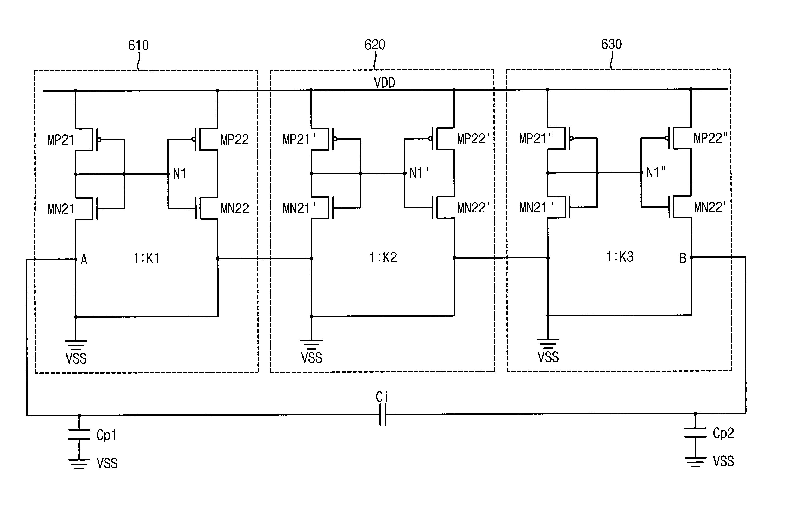
[0045]FIG. 6 shows a block diagram of a capacitance multiplier according to an embodiment of the present invention. Referring to FIG. 6, the capacitance multiplier includes a current amplifying circuit 600 and a capacitor Ci. The current amplifying circuit 600 includes a plurality of current amplifiers such as first, second, and nth current amplifiers 610, 620, . . . , and 630.

[0046]The current amplifiers 610, 620, . . . , and 630 are cascaded in series, and each of the current amplifiers 610, 620, . . . , and 630 has a respective current gain K1, K2, . . . , Kn. In addition, the capacitor Ci is coupled in parallel across the cascade of the current amplifiers 610, 620, . . . , and 630.

[0047]FIG. 7 shows a circuit diagram of a current amplifier included in the capacitance multiplier of FIG. 6 according to an exemplary embodiment of the present invention. Referring to FIG. 7, the current amplifier includes PMOSFETs (P-channel metal oxide semiconductor field effect transistors) MP21 an...


PUM


Abstract

A capacitance multiplier includes a cascade of a plurality of current amplifiers with each current amplifier having a respective current gain Ki. In addition, the capacitance multiplier includes a capacitor coupled in parallel across the cascade of current amplifiers. Such a capacitance multiplier occupies a smaller area with higher capacitance gain but with low power consumption.

Description

BACKGROUND OF THE INVENTION[0001]This application claims priority to Korean Patent Application No. 2004-43670 filed on Jun. 14, 2004 in the Korean Intellectual Property Office, the entire contents of which are hereby incorporated by reference.[0002]1. Field of the Invention[0003]The present invention relates generally to a capacitance multiplier, and in particular to a capacitance multiplier with cascaded current amplifiers for enhanced capacitance gain and low power consumption.[0004]2. Description of the Related Art[0005]A PLL (Phase Locked Loop) is commonly used for communication, multimedia, and other applications. FIG. 1 is a block diagram of a conventional PLL (Phase Locked Loop). Referring to FIG. 1, the PLL includes a PFD (Phase Frequency Detector) 100, a charge pump 200, a loop filter 300, a VCO (voltage controlled oscillator) 400, and a frequency divider 500.[0006]The PFD 100 generates an up signal SUP and / or a down signal SDN based on a phase (and frequency) difference be...

Claims


Application Information

Patent Timeline
Patent Type & Authority Patents(United States)
IPC IPC(8): H03L7/06H03L7/08H03H11/48H03L7/089H03L7/093
CPCH03H11/48H03H11/483H03L7/093H03L7/0891H03L7/08
Inventor KIM, JAE-WAN
Owner SAMSUNG ELECTRONICS CO LTD
Why Eureka
Try Eureka