Chip resistor having low resistance and method of making the same

a technology of resistor and chip, which is applied in the manufacture of resistor chips, resistors adapted for the application of terminals, resistor details, etc., can solve the problems of producing a change in resistance and increasing manufacturing costs, so as to reduce the overall height of the chip resistor, increase the height of the connection terminal electrode, and reduce the weight

Inactive Publication Date: 2007-05-22
ROHM CO LTD
View PDF6 Cites 18 Cited by
  • Summary
  • Abstract
  • Description
  • Claims
  • Application Information

AI Technical Summary

Benefits of technology

[0012]In this way, by covering with an insulator at least the portion between the two connection terminal electrodes in the lower surface of the resistor elements comprised by the metal plate, it is possible to use this insulator to prevent contact of molten solder with the portion between the two connection terminal electrodes in the resistor element when soldering onto a printed circuit board or the like. Consequently, since it is unnecessary to increase the height of the connection terminal electrodes in order to avoid contact of the molten solder, the overall height in the chip resistor can be made correspondingly lower and a reduction in weight thereby achieved.
[0022]In particular, as described in claim 7, by covering the upper surface of the metal plate blank with an insulator, in the plating step of forming a plating layer for soldering on the lower surface of the metal plate blank, the formation of a plating layer on the upper surface on the blank substrate can be prevented by the insulator that covers this upper surface. In other words, the insulator that covers the upper surface of the resistor element in the chip resistor can be utilized as a mask formed beforehand on this upper surface for preventing formation of a plating layer on this upper surface in the plating step. Thus, the advantages are obtained that the plating step is simplified and manufacturing costs can be further reduced.

Problems solved by technology

However, with the chip resistor 1 of the prior art, there is a considerable risk that, when soldering onto the printed circuit board or the like, molten solder will become attached to portions between the two connection terminal electrodes 4, 5 on the resistor element 2 beyond the two connection terminal electrodes 4, 5, thereby producing a change in the resistance.
In this manner, the manufacturing costs can be greatly increased due to the need for a step of forming a resist mask for partial plating beforehand on the lower surface of the metal plate blank prior to the plating step of forming the plating layers 6, 7 for the soldering, and also a step of separating and removing the resist mask for the partial plating after the plating step.

Method used


Image

  • Chip resistor having low resistance and method of making the same
  • Chip resistor having low resistance and method of making the same
  • Chip resistor having low resistance and method of making the same

Examples


first embodiment

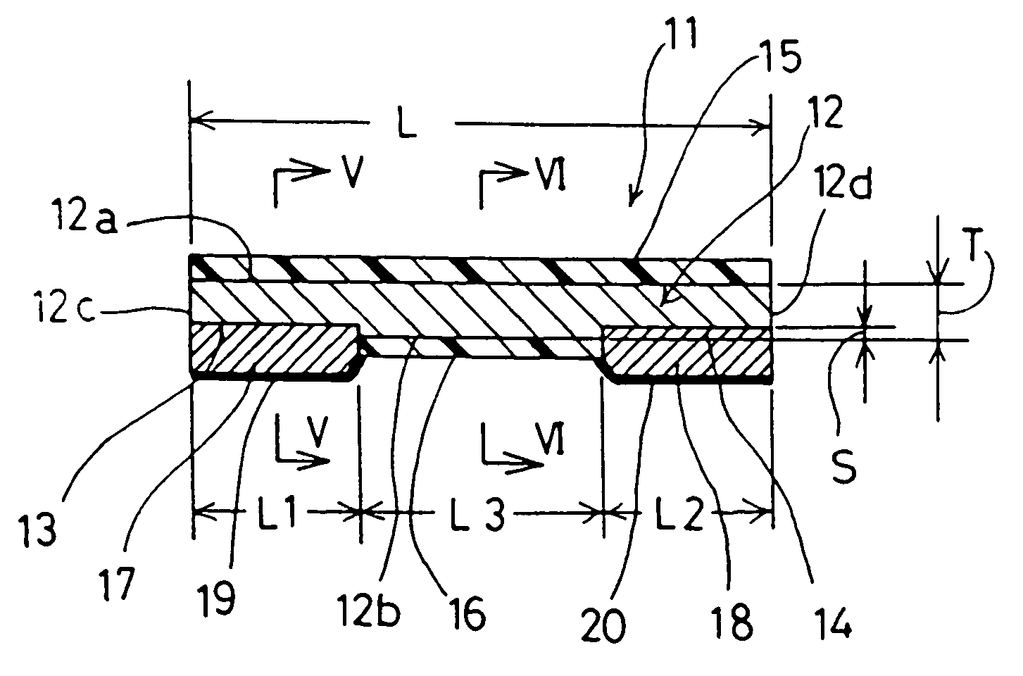
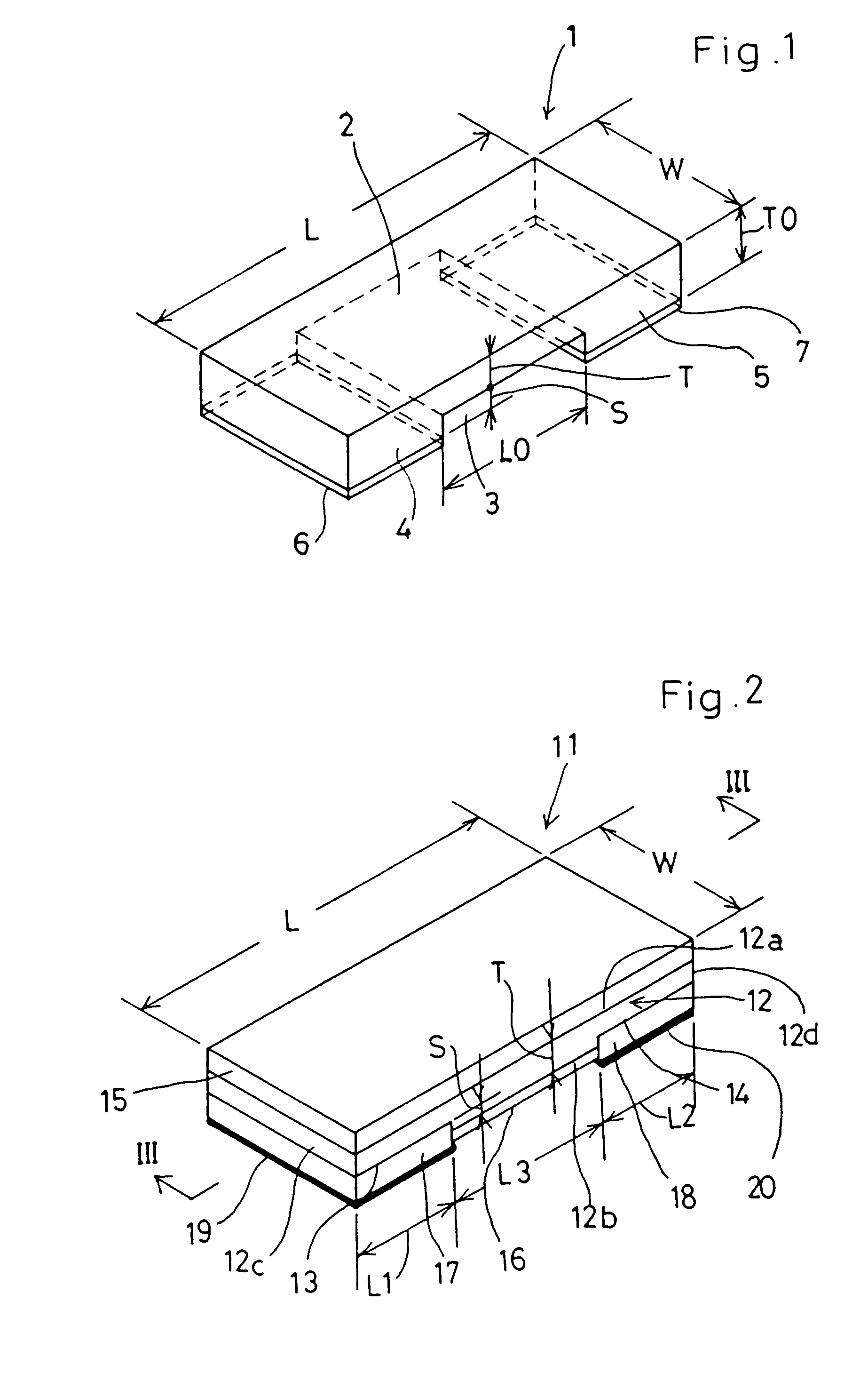
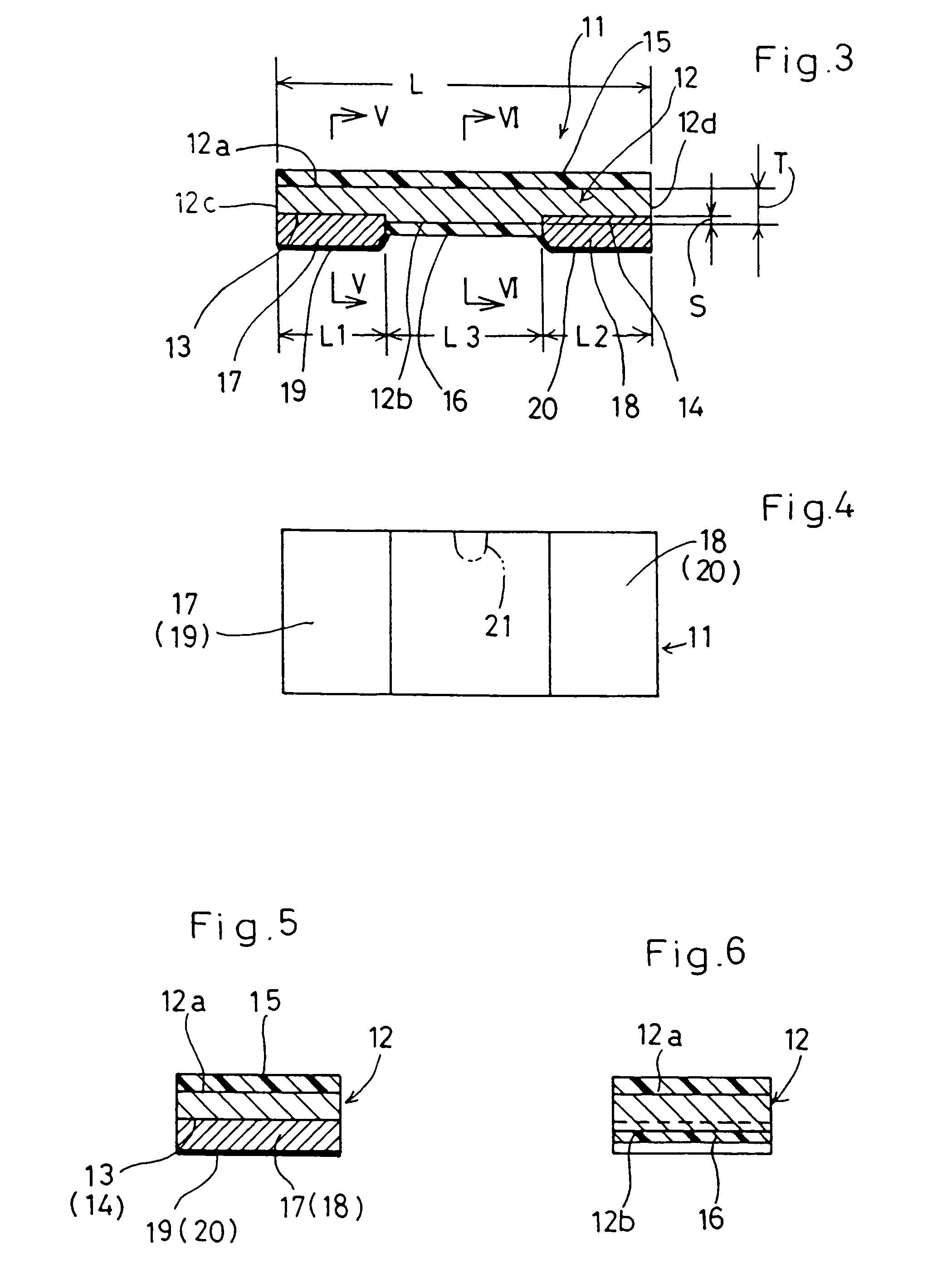
[0048]the present invention is described below with reference to FIG. 2 to FIG. 6. In these Figures, the reference symbol 11 indicates a chip resistor according to an embodiment of the present invention.

[0049]This chip resistor 11 comprises a resistor element 12 formed in rectangular shape of length L and width W.

[0050]This resistor element 12 is made of metal plate of thickness T. The metal used is for example alloy such as copper-nickel alloy, nickel-chromium alloy or iron-chromium alloy in which metal (hereinafter called a high-resistant metal) having a higher resistance than a metal substrate is added to the substrate, which is made of a metal having a lower resistance (hereinafter called low-resistant metal).

[0051]In portions at the two ends of the lower surface of 12b, of the upper and lower surfaces 12a and 12b of the resistor element 12, recesses 13 and 14 are cut which are respectively of length L1, L2 from the two end faces 12c, 12d of this resistor element 12, and of dept...

second embodiment

[0074]Next, the present invention will be described with reference to FIG. 16 to FIG. 20.

[0075]In these Figures, the reference symbol 111 indicates a chip resistor according to the second embodiment of the present invention.

[0076]This chip resistor 111 comprises a resistor element 112 that is formed in a rectangular shape with a length L and a width W.

[0077]This resistor element 112 is made of metal plate of thickness T. The metal used is for example alloy such as copper-nickel alloy, nickel-chromium alloy or iron-chromium alloy in which metal (hereinafter called a high-resistant metal) having a higher resistance than a substrate is added to the substrate, which is made of a metal having a lower resistance (hereinafter called low-resistant metal).

[0078]Connection terminal electrodes 117, 118 are formed at portions at the two ends thereof by cutting a recess 113 of length L0 and depth S in the lower surface of the upper and lower surfaces of the resistor element 112, in about the mid...


PUM

PropertyMeasurementUnit
resistanceaaaaaaaaaa
insulatingaaaaaaaaaa
thickness T0aaaaaaaaaa

Abstract

A resistor, including a resistive element made of a metal plate, has a low resistance resulting from connection terminal electrodes formed on both ends of the lower surface of the resistive element. The object thereof is to achieve weight reduction and lower costs by reducing the height of the resistor. To achieve the above object, the ends of the lower surface of the resistive element are provided with recesses for accommodating the connection terminal electrodes, while at least the intermediate area of the lower surface of the resistive element between the connection terminal electrodes is covered with an insulator. Alternatively, a recess may be formed in the middle of the lower surface of the resistive element for using the ends of the lower surface as a pair of connection terminal electrodes, the recess being internally covered with an insulator.

Description

BACKGROUND OF THE INVENTION[0001]The present invention relates to a chip resistor having a low resistance of, for example, no more than 1 Ω, and to a method of making the same.[0002]As a prior art document, JP-A-2001-118701 proposes a chip resistor 1 constructed as shown in FIG. 1.[0003]Specifically, the resistor element 2 of a chip resistor 1 of the prior art is formed in rectangular shape of metal plate of thickness T0, length L and width W, and made of a material such as an alloy constituted by adding metal having higher resistance such as nickel to a substrate metal having a low resistance such as copper. Connection terminal electrodes 4, 5 are provided in portions at the left and right ends of the lower surface of this resistor element 2, by using cutting processing to cut a recess 3 of length L0 and depth S in about the middle of the lower surface of this resistor element 2. In addition, plating layers 6, 7 are formed on these two connection terminal electrodes 4 and 5 in orde...

Claims


Application Information

Patent Timeline
Patent Type & Authority Patents(United States)
IPC IPC(8): H01C1/012H01C1/142H01C7/00H01C17/00H01C17/28
CPCH01C1/142H01C7/003H01C17/281H01C17/006Y10T29/49082
Inventor TSUKADA, TORAYUKI
Owner ROHM CO LTD
Why Eureka
Try Eureka