Method of forming a semiconductor arrangement with reduced field-to active step height

a semiconductor and step height technology, applied in semiconductor/solid-state device manufacturing, basic electric elements, electric devices, etc., can solve problems such as “stringer” defects, photolithographic patterning or etch considerations, and pattern integrity issues of polysilicon gate patterns, and achieve the effect of reducing the step heigh

Inactive Publication Date: 2007-05-29
ADVANCED MICRO DEVICES INC
View PDF8 Cites 2 Cited by
  • Summary
  • Abstract
  • Description
  • Claims
  • Application Information

AI Technical Summary

Benefits of technology

[0007]This and other needs are met by embodiments of the present invention which provide a method of forming a semiconductor arrangement comprising the steps of forming a substrate with a top surface, active regions and field oxide regions. The field oxide regions have portions that extend above the top surface of a substrate and the active regions by a step height. The portions of the field oxide regions that extend above the top surface and the active regions are then removed. In certain embodiments of the invention, the method includes forming a dielectric layer over the field oxide regions and the active regions and then performing a chemical mechanical polishing or blanket etch back to planarize the structure. This reduces the field-to-active step height differential, and also reduces or eliminates the impact of a divot in the field oxide that can be created.

Problems solved by technology

The difference in height between the top surface of the STI region 12 and the top surface of the silicon substrate 10 can result in problems in the photolithographic patterning or etch considerations.
In other words, the height of the step can cause pattern integrity issues of the polysilicon gate.
Additionally, if the step is excessive, polysilicon material can be trapped along the step to thereby cause “stringer” defects.
Hence, undesirable height of the step may produce pattern integrity issues that reduce the quality of the semiconductor device that is ultimately produced.

Method used


Image

  • Method of forming a semiconductor arrangement with reduced field-to active step height
  • Method of forming a semiconductor arrangement with reduced field-to active step height
  • Method of forming a semiconductor arrangement with reduced field-to active step height

Examples


Embodiment Construction

[0014]The present invention addresses problems related to the step height created during STI formation and polishing in conventional STI formation methodologies. This reduction in the step height is achieved by the formation of a planarizing dielectric layer on the substrate and the field oxide, followed by a planarization step. This reduces or eliminates the field-to-active step height prior to the gate oxidation and polysilicon deposition steps in the semiconductor manufacturing process. This has a desirable effect on the photolithographic patterning and etch steps to improve pattern integrity and increase operating speed, with also improved yield and precision in formation.

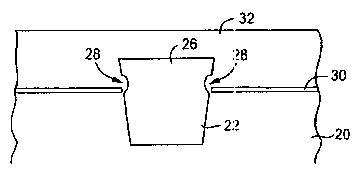
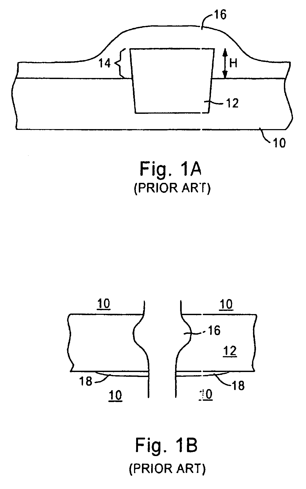
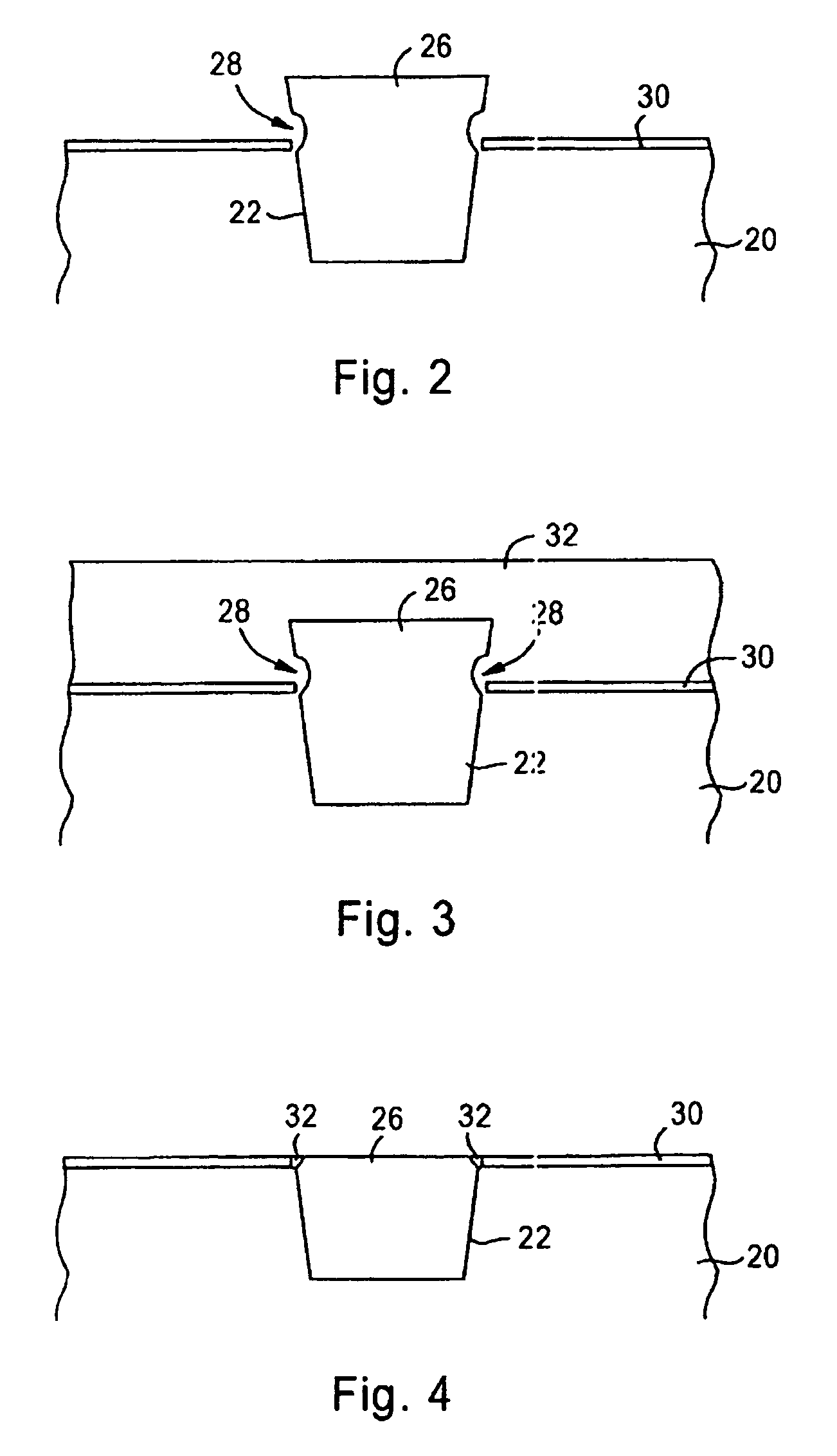
[0015]FIG. 2 schematically depicts a cross-section of a portion of a semiconductor wafer during formation of an STI arrangement in accordance with embodiments of the present invention. A silicon substrate 20 is provided with a trench 22 that has been filled with a suitable insulating (or isolating) material 26 ...


PUM


Abstract

A method of forming a shallow trench isolation (STI) region in a silicon substrate creates an STI region that extends above a top surface of the silicon substrate. A planarizing dielectric layer is formed on the substrate and extends above the field oxide regions. The planarizing dielectric layer is removed by chemical mechanical polishing or blanket etch back, for example, as well as those portions of the field oxide regions that extend above the top surface of the substrate and the active regions. The step height is thereby eliminated or significantly reduced.

Description

FIELD OF THE INVENTION[0001]The present invention relates to semiconductor processing, and more particularly, to formation of shallow trench isolation (STI) regions.BACKGROUND OF THE INVENTION[0002]An important aim of on-going research in the semiconductor industry is increasing semiconductor performance while decreasing power consummation in the semiconductor devices. Planar transistors, such as metal-oxide semiconductor field effect transistors (MOSFETs), are particularly well-suited for use in high-density integrated circuits. As the size of MOSFETs and other devices decrease, the dimensions of source / drain regions, channel regions, and gate electrodes of the devices, also decrease. One of the techniques to shrink device sizes is that of shallow trench isolation (STI). The use of STI significantly shrinks the area needed to isolate the transistors better than the local oxidation of silicon (LOCOS) technique. STI provides superior latch-up immunity, smaller channel width encroachm...

Claims


Application Information

Patent Timeline
Patent Type & Authority Patents(United States)
IPC IPC(8): H01L21/311
CPCH01L21/76232
Inventor BONSER, DOUGLAS J.DAKSHINA-MURTHY, SRIKANTESWARAKELLING, MARK C.PELLERIN, JOHN G.GROSCHOPF, JOHANNES F.NOMURA, EDWARD ASUKA
Owner ADVANCED MICRO DEVICES INC
Why Eureka
Try Eureka