Chip package with embedded panel-shaped component

a panel-shaped component and chip technology, applied in the field of chip packages, can solve the problems of increasing serious cross-talk at high-frequency transmission and too long signal transmission pathways, and achieve the effect of improving electrical performance and increasing heat dissipation capacity

Active Publication Date: 2007-05-29
VIA TECH INC
View PDF17 Cites 71 Cited by
  • Summary
  • Abstract
  • Description
  • Claims
  • Application Information

AI Technical Summary

Benefits of technology

[0010]Accordingly, at least one objective of the present invention is to provide a bump-less chip package having better electrical performance and higher heat-dissipating capacity.
[0012]According to the present invention, the chip is disposed on the panel-shaped component, which has great heat-dissipating capacity. Thus, heat generated by the chip can be rapidly transmitted to the panel-shaped component and hence the bump-less chip package has a higher heat-dissipating capacity. Furthermore, if the panel-shaped component is a capacitor or other type of passive component, the bump-less chip package can have even better electrical performance. Moreover, the panel-shaped component can be another chip so that the package becomes a stacked bump-less multi-chip package.

Problems solved by technology

However, since the conventional BGA packaging technique requires a high layout density package substrate, together with a flip-chip bonding or wire bonding electrical connection, signal transmission pathway becomes too long.
Although the conventional bump-less build-up layer chip package 100 has good reliability and high electrical performance, the problem of cross talk at high frequency transmission is increasingly serious due to increased circuit layout density and reduced line pitch.

Method used


Image

  • Chip package with embedded panel-shaped component
  • Chip package with embedded panel-shaped component
  • Chip package with embedded panel-shaped component

Examples


first embodiment

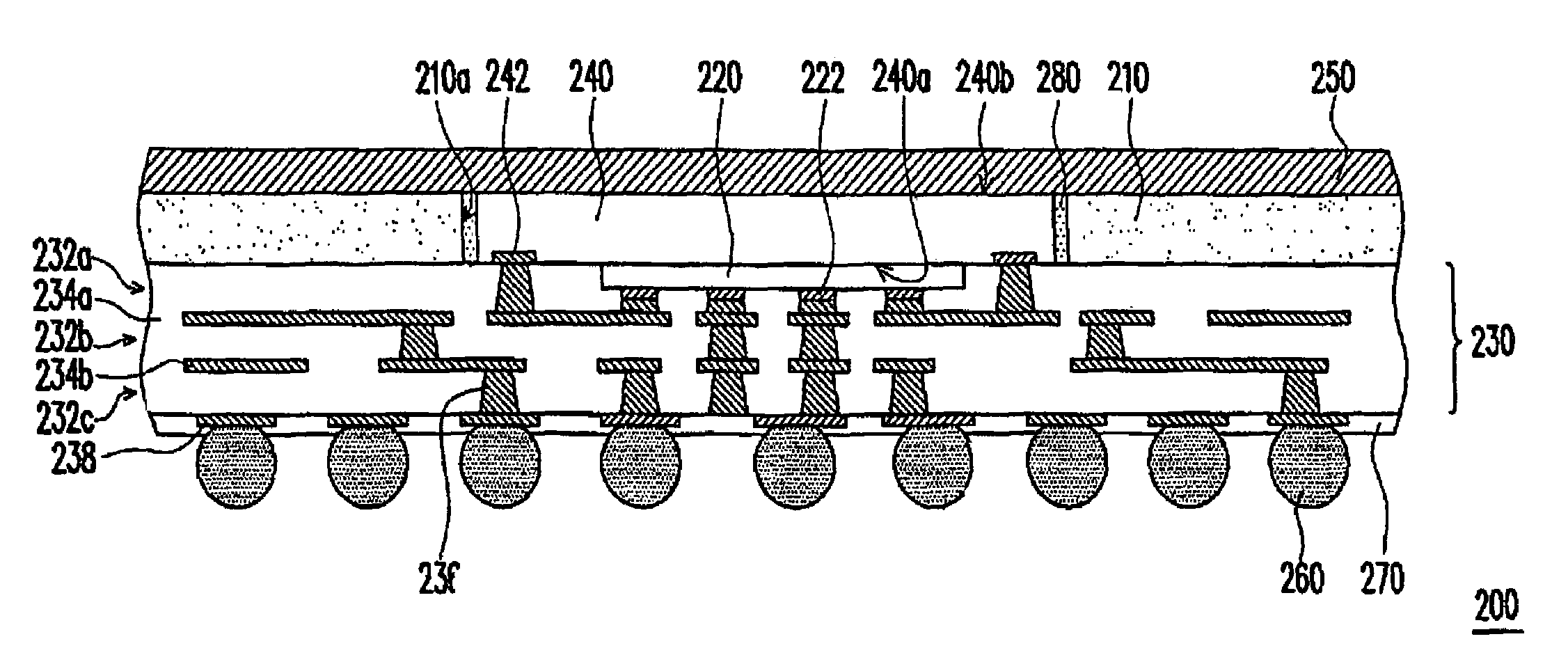
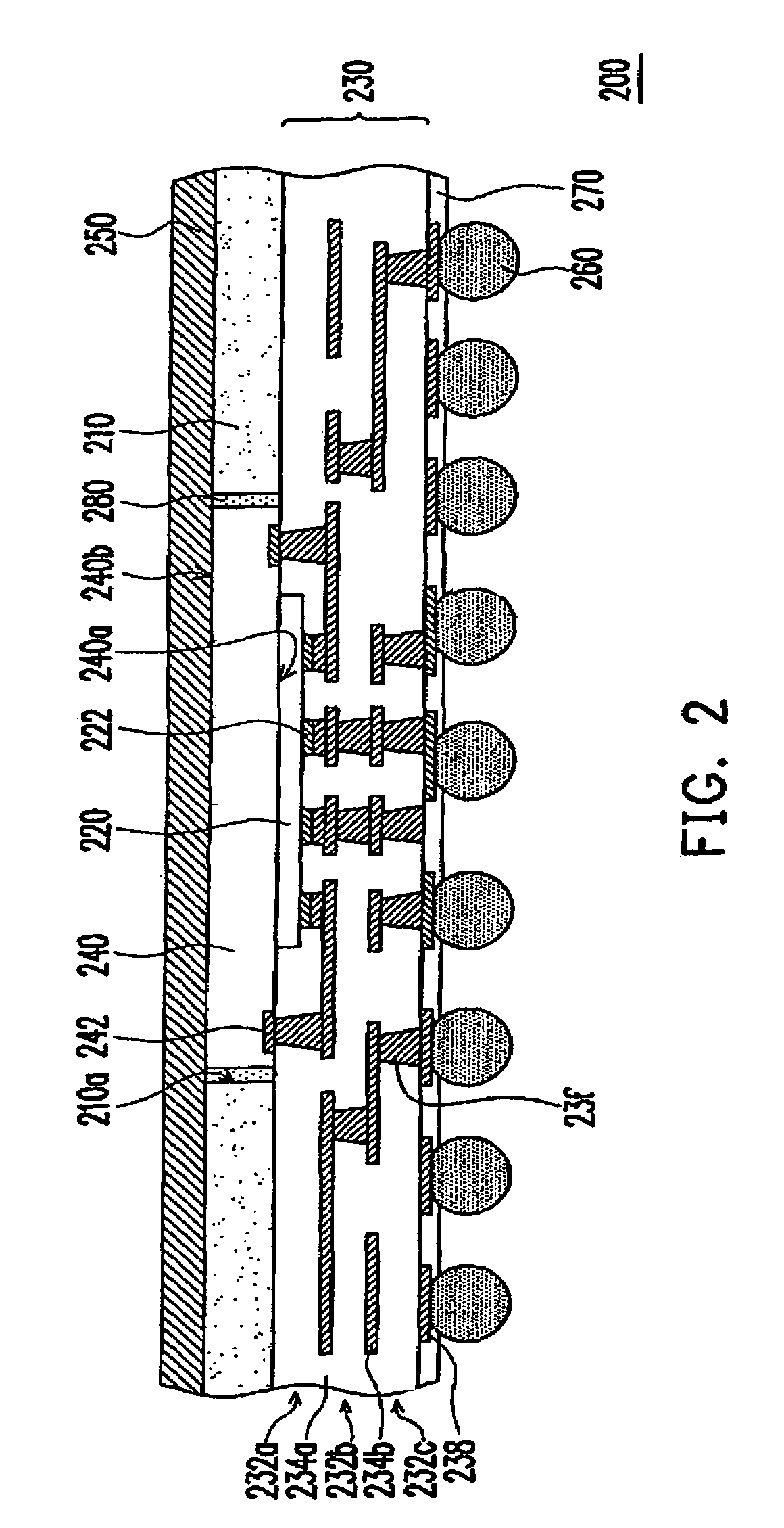
[0020]FIG. 2 is a schematic cross-sectional view of a bump-less chip package according to a first embodiment of the present invention. As shown in FIG. 2, the bump-less chip package 200 in the present embodiment comprises a stiffener 210, a chip 220, an interconnection structure 230 and a panel-shaped component 240. The stiffener 210 has at least one opening 210a. The panel-shaped component 240 is embedded within the opening 210a. In addition, the panel-shaped component 240 has a plurality of electrical terminals 242, such as electrodes or conductive pads, on a first surface 240a thereof. It should be noted that for the panel-shaped component 240 to be fixed inside the opening 210a, some encapsulating material 280 is filled between the panel-shaped component 240 and the stiffener 210. The stiffener 210 is fabricated using a material such as glass or metal. However, the stiffener 210 may be fabricated using other dielectric material or conductive material.

[0021]The back surface of th...

second embodiment

[0028]FIG. 3 is a schematic cross-sectional view of a bump-less chip package according to a second embodiment of the present invention. As shown in FIG. 3, the second embodiment is very similar to the first embodiment except that the bump-less chip package 300 in the second embodiment, the size of panel-shaped component 210 is substantially identical to that of the interconnection structure 230 so that the panel-shaped component 210 can be regarded as a carrier for carrying the chip 220 and the interconnection structure 230 is disposed on the chip 220 and the panel-shaped component 310. In other words, the present embodiment does not have a similar structure to the stiffener 210 and the encapsulating material 280 in FIG. 2. Furthermore, the electrical terminals 312 of the panel-shaped component 310 can have different pattern arrangement, such as a surface array, concentric rings or other type of organization.

[0029]Similarly, the panel-shaped component 310 can be a panel-shaped activ...


PUM


Abstract

A bump-less chip package is provided. The bump-less chip package includes a chip, an interconnection structure and a panel-shaped component. The panel-shaped component has a plurality of electrical terminals on a first surface thereof. The back surface of the chip is disposed on the first surface of the panel-shaped component, and the chip has a plurality of first pads on the active surface thereof away from the panel-shaped component. The interconnection structure is disposed on the first surface of the panel-shaped component and the active surface of the chip. The first pads of the chip may electrically connect with the electrical terminals of the panel-shaped component through the interconnection structure. Furthermore, the interconnection structure has a plurality of second pads on the surface away from the chip.

Description

CROSS-REFERENCE TO RELATED APPLICATION[0001]This application claims the priority benefit of Taiwan application serial no. 94101768, filed on Jan. 21, 2005. All disclosure of the Taiwan application is incorporated herein by reference.BACKGROUND OF THE INVENTION[0002]1. Field of the Invention[0003]The present invention relates to a chip package. More particularly, the present invention relates to a bump-less build-up layer (BBUL) type of chip package.[0004]2. Description of the Related Art[0005]With the rapid development of new electronic technologies, the electronic devices have developed to have higher processing speed, multi-function, high integration, miniaturized size and low cost. As a result, chip packaging is also developing towards miniaturization and densification. The conventional ball grid array (BGA) packaging technique often utilizes a package substrate to serve as a carrier for an integrated circuit (IC) chip and then applies flip-chip bonding or a wire bonding method t...

Claims


Application Information

Patent Timeline
Patent Type & Authority Patents(United States)
IPC IPC(8): H01L23/52H01L23/48
CPCH01L23/49816H01L23/5389H01L2224/73204
Inventor HSU, CHI-HSING
Owner VIA TECH INC
Why Eureka
Try Eureka