Driving circuit system for use in electro-optical device and electro-optical device

a technology of driving circuit and electrooptical device, which is applied in the direction of digital storage, instruments, computing, etc., can solve the problems of relatively complicated active elements, and achieve the effect of simple circuit configuration, simple circuit configuration, and easy reduction of the circuit pitch of the first and second output circui

Inactive Publication Date: 2007-05-29
138 EAST LCD ADVANCEMENTS LTD
View PDF34 Cites 24 Cited by
  • Summary
  • Abstract
  • Description
  • Claims
  • Application Information

AI Technical Summary

Benefits of technology

[0055]According to one aspect of the fifth driving circuit system for use in the electro-optical device, the first output circuit may comprise a first branching wiring pattern, provided in correspondence with each of the unit circuits, for branching the transfer signal output from the corresponding unit circuit into the plurality of transfer signal components, and a first enable circuit, provided in correspondence with each of the transfer signal components branched by the first branching wiring pattern, for outputting an AND signal of the transfer signal component branched by the first branching wiring pattern and an enable signal belonging to a first group. The enable signals belonging to the first group whose active periods do not overlap with each other during a cycle in which the transfer signal components branched by the same first branching wiring pattern are supplied are individually supplied to the first enable circuits to which the transfer signal components branched by the same first branching wiring pattern are supplied. The second output circuit may comprise a second branching wiring pattern, provided in correspondence with each of the first enable circuits, for branching each of the transfer signal components divided by the corresponding first enable circuit into the plurality of transfer signal portions, and a second enable circuit, provided in correspondence with each of the transfer signal portions branched by the second branching wiring pattern, for outputting as a sampling control signal an AND signal of the transfer signal portion branched by the second branching wiring pattern and an enable signal belonging to a second group. When the transfer signal component is divided into the plurality of transfer signal portions in the time domain, the enable signals belonging to the second group whose active periods do not overlap with each other during a cycle in which the transfer signal portions branched by the same second branching wiring pattern are supplied are individually supplied to the second enable circuits to which the transfer signal portions branched by the same se

Problems solved by technology

However, each unit circuit of the above-described shift registers is

Method used


Image

  • Driving circuit system for use in electro-optical device and electro-optical device
  • Driving circuit system for use in electro-optical device and electro-optical device
  • Driving circuit system for use in electro-optical device and electro-optical device

Examples


first embodiment

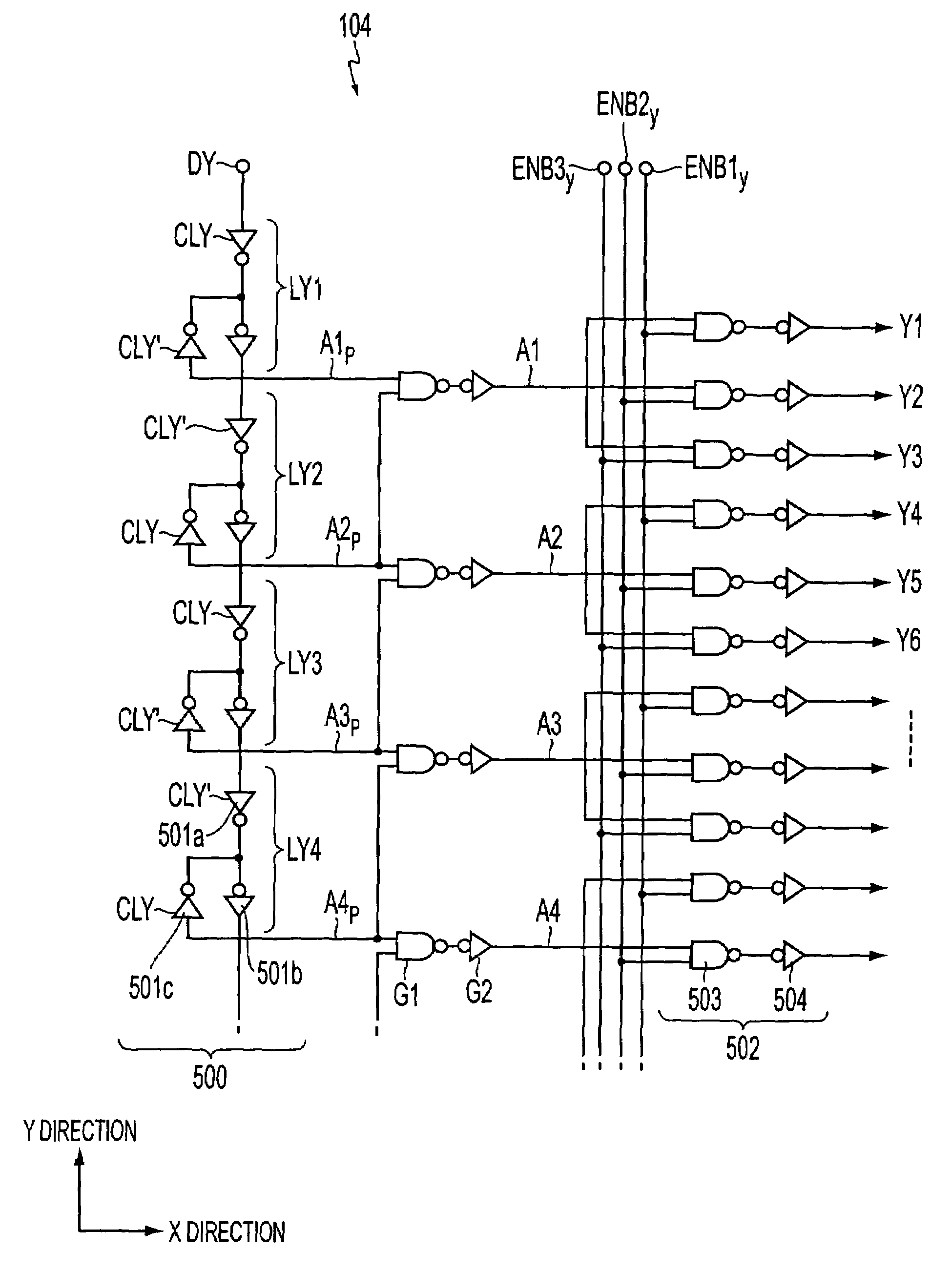
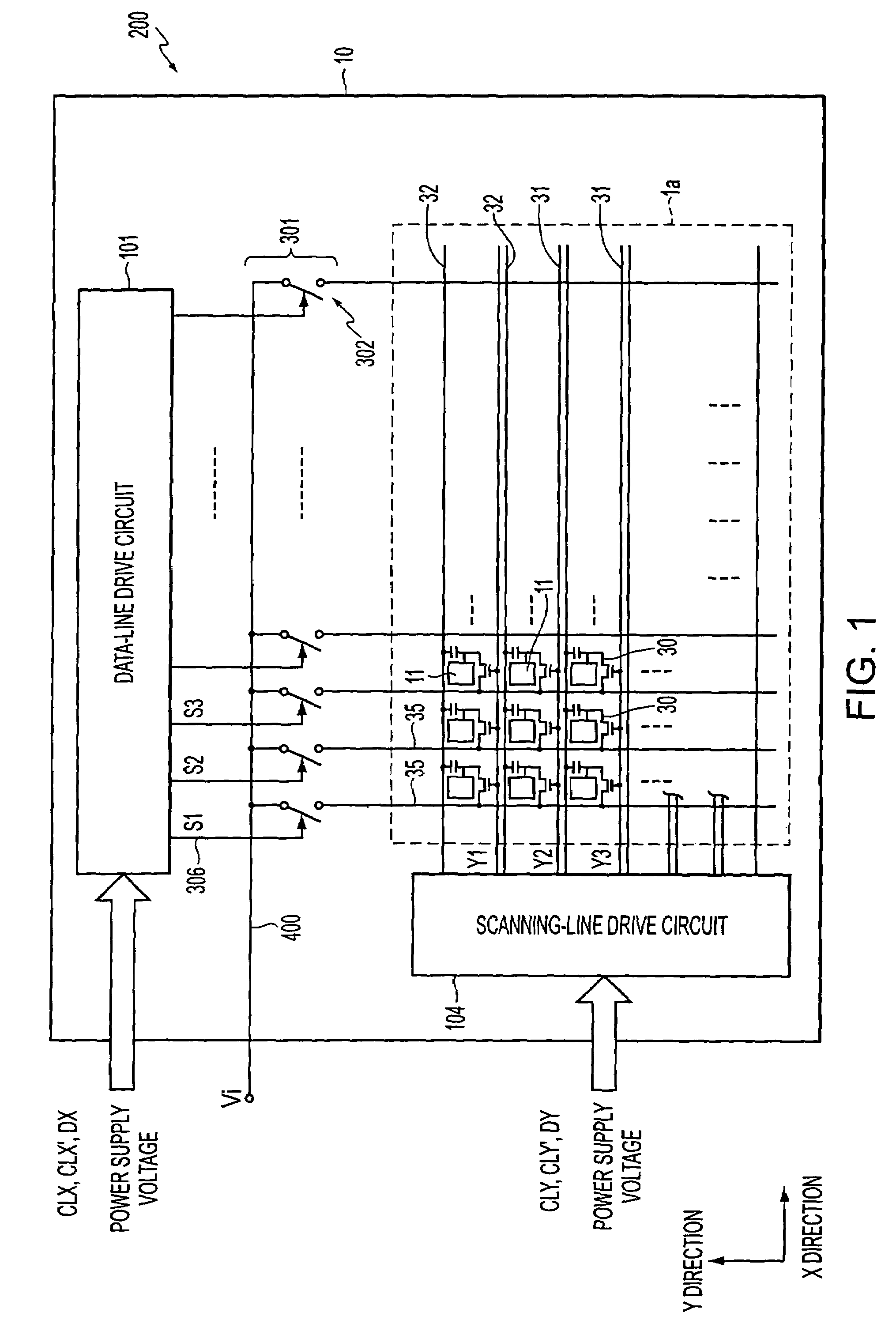
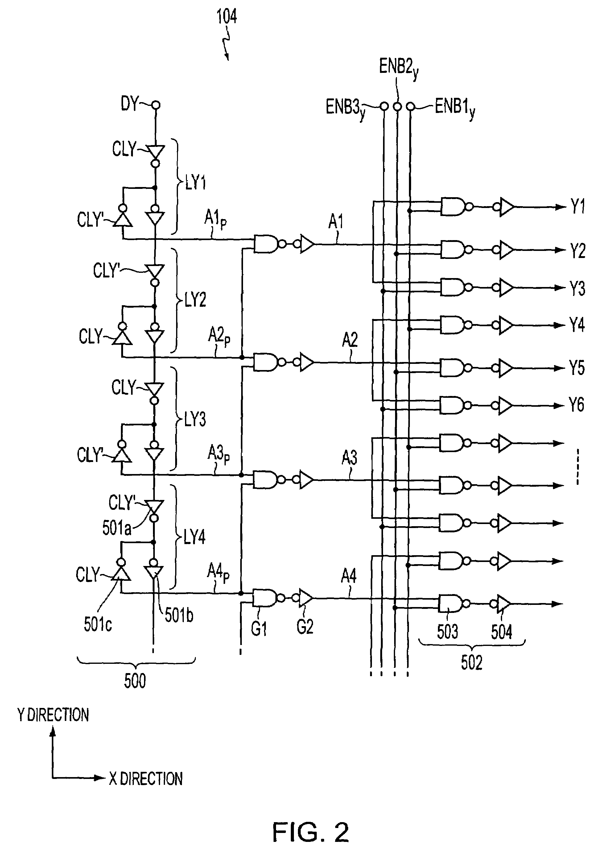
[0079]A description is first given of a FIG. 1 is a block diagram illustrating the entire configuration of an electro-optical device provided with a driving circuit system of this embodiment on a substrate. In this figure, a liquid crystal device 200 includes a liquid crystal display portion 1a, a data-line driving circuit 101, a scanning-line driving circuit 104, a sampling circuit 301, and so on.

[0080]Among the above-described elements, the data-line driving circuit 101, the scanning-line driving circuit 104, and the sampling circuit 301 are provided at the peripheral portion of the liquid crystal display portion 1a on a TFT array substrate 10, formed of, for example, a quartz substrate, hard glass, or a silicon substrate. On the liquid crystal display portion 1a on the TFT array substrate 10, a plurality of data lines 35 are formed parallel to each other in the Y direction, as viewed from FIG. 1, while a plurality of scanning lines 31 are formed in the X direction, as viewed fro...

third embodiment

[0137]As described above, in the liquid crystal device when being operated in the first mode, the image signal is sampled onto each of the data lines 35, thereby sequentially driving the corresponding pixel portions.

[0138]The display operation performed in accordance with the second operation mode is as follows. In the second operation mode, the following enable signals ENB1x, ENB2x, and ENB3x are supplied to the corresponding enable circuit 602 (see FIG. 7). More specifically, as illustrated in FIG. 13, the enable signals ENB1x, ENB2x, and ENB3x have a frequency twice as high as the clock signal CLX (inverted clock signal CLX′). The pulse widths of the enable signals ENB1x, ENB2x, and ENB3x are shorter than that of the clock signal CLX (inverted clock signal CLX′), and the pulse-width cycles of the enable signals ENB1x, ENB2x, and ENB3x are in phase.

[0139]Thus, since the transfer signal B1 output from the initial-stage inverter G4 is simultaneously distributed in accordance with t...

fourth embodiment

[0174]According to the foregoing description, in the fourth embodiment, the transfer signal output in correspondence with each unit circuit of the X-direction shift register 600 is first sequentially divided into two components in the time domain by the first enable circuit 612, thereby obtaining two signals without overlap of the pulse widths. Between the two signals, in the first mode, one of the signals is sequentially divided into three portions in the time domain by the second enable circuits 622, thereby obtaining three sampling signals without overlap of the pulse widths. In the second mode, however, one of the two signals is simultaneously distributed into three portions by the second enable circuits 622, thereby acquiring the three sampling signals of the same type having the same pulse width.

[0175]The writing operation performed by sequential driving in the first operation mode, and the writing operation performed by simultaneous-multiple driving in the second operation mo...


PUM


Abstract

An electro-optical device copes with a decreased size of a pixel pitch by using a comparatively simple configuration in which a driving circuit system is formed on one substrate. In a scanning-line driving circuit, each transfer signal of a shift register is branched off into three signal components, and an enable circuit is provided for each signal component. During a pulse cycle of the transfer signal, one transfer signal is divided into three components while being sequentially shifted in the time domain in accordance with enable signals whose phases are sequentially shifted from each other, and the divided components are output as scanning signals. The same applies to a data-line driving circuit.

Description

[0001]This a Divisional of U.S. patent application Ser. No. 09 / 362,654, filed on Jul. 29, 1999, now U.S. Pat. No. 6,670,943 the contents of which are incorporated herein in its entirety.BACKGROUND OF THE INVENTION[0002]1. Field of Invention[0003]The present invention relates to a driving circuit system for use in an active-matrix-type electro-optical device and for driving the electro-optical device, and also to an electro-optical device driven by this driving circuit system.[0004]2. Description of Related Art[0005]Generally, in an active matrix type electro-optical device, a plurality of scanning lines and a plurality of data lines are arranged in a matrix, and pixel electrodes are formed via switching elements, such as thin film diodes (hereinafter referred to as “TFDs”) and thin film transistors (hereinafter referred to as “TFTs”) in correspondence with the intersections of the matrix.[0006]In the electro-optical device configured as described above, scanning signals are sequenti...

Claims


Application Information

Patent Timeline
IPC IPC(8): G09G3/36G02F1/133G02F1/136G02F1/1368G09G3/20
CPCG09G3/3677G09G3/3688G09G2300/0408G09G2310/0297G09G3/20
Inventor ISHII, KENYAUCHIDA, MASAHIDE
Owner 138 EAST LCD ADVANCEMENTS LTD
Why Eureka
Try Eureka