Semiconductor devices and semiconductor device components with peripherally located, castellated contacts, assemblies and packages including such semiconductor devices or packages and associated methods

a technology of semiconductor devices and semiconductor devices, applied in the direction of printed circuit manufacturing, printed circuit electric connection formation, printed circuit aspects, etc., can solve the problems of large footprint device, large footprint device, and inconvenient use and achieve the effect of reducing the thickness of conventional flip-chip type packages

Inactive Publication Date: 2007-06-05
MICRON TECH INC
View PDF82 Cites 16 Cited by
  • Summary
  • Abstract
  • Description
  • Claims
  • Application Information

AI Technical Summary

Problems solved by technology

As with the flat packages, conventional flip-chip type packages are often undesirably thick for use in small, thin, state of the art electronic devices.
Furthermore, use of this general construction method for producing a stacked multichip module (MCM) results in a relatively high-profile, large footprint device.
While interposers that include recesses for partially receiving semiconductor devices facilitate the fabrication of thinner flip-chip type packages, the semiconductor dice of these packages, as well as intermediate conductive elements that protrude beyond the outer surfaces of either the semiconductor dice or the interposers, undesirably add to the thicknesses of these packages.
While this method results in a very low-profile flip-chip type package, the package cannot be tested separately from the carrier substrate.
As a result, if the package is unreliable, it may also be necessary to discard the carrier substrate and any other components thereon.
Moreover, the packaging method of the '695 Patent complicates the process of connecting semiconductor devices and other electronic components to a carrier substrate.
In addition, it should be noted that in order to obtain a low-profile package, it may be necessary to sacrifice footprint compactness.

Method used


Image

  • Semiconductor devices and semiconductor device components with peripherally located, castellated contacts, assemblies and packages including such semiconductor devices or packages and associated methods
  • Semiconductor devices and semiconductor device components with peripherally located, castellated contacts, assemblies and packages including such semiconductor devices or packages and associated methods
  • Semiconductor devices and semiconductor device components with peripherally located, castellated contacts, assemblies and packages including such semiconductor devices or packages and associated methods

Examples


Embodiment Construction

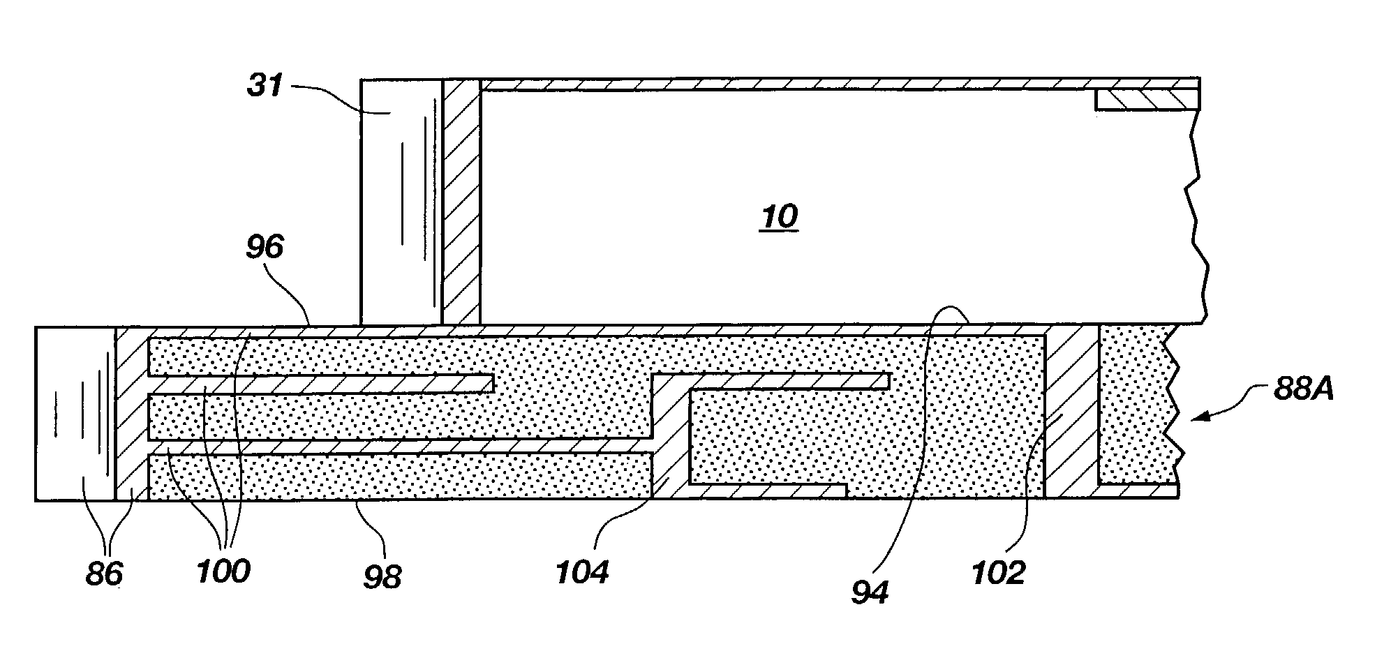
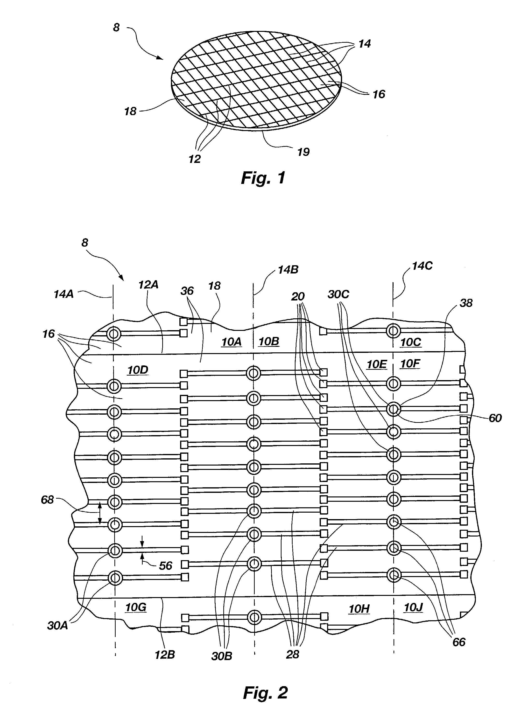
[0037]Referring to FIG. 1, a multichip substrate blank 8 is shown in which a plurality of dice 16 is shown as defined by boundary lines 12 and 14. In accordance with the invention, semiconductor device packages will be formed on the dice 16 in a manner which facilitates the stacking of the packages in a low-profile, small footprint multichip assembly. While substrate blank 8 depicted as comprising a full silicon wafer, use of other semiconductor substrates (e.g., partial wafers, substrates of other semiconductive materials, including, without limitation, gallium arsenide indium phosphide, and the like, as well as so-called silicon-on insulator, or SOI, type substrates) is also within the scope of the present invention.

[0038]The initial processes in forming package 10 may be any of those well-known and used throughout the industry. Thus, one side of the substrate blank 8 is selected as an active surface 18; the opposite side becomes the back side 19.

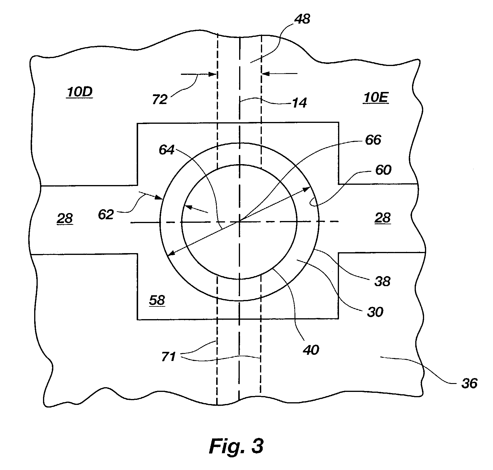
[0039]A pattern of planned straigh...


PUM


Abstract

A multichip assembly includes semiconductor devices or semiconductor device components with outer connectors on peripheral edges thereof. The outer connectors are formed by creating via holes along boundary lines between adjacent, unsevered semiconductor devices, or semiconductor device components, then plating or filling the holes with conductive material. When adjacent semiconductor devices or semiconductor device components are severed from one another, the conductive material in each via between the semiconductor devices is bisected. The semiconductor devices and components of the multichip assembly may have different sizes, as well as arrays of outer connectors with differing diameters and pitches. Either or both ends of each outer connector may be electrically connected to another aligned outer connector or contact area of another semiconductor device or component. Assembly in this manner provides a low-profile stacked assembly.

Description

CROSS-REFERENCE TO RELATED APPLICATION[0001]This application is a divisional of application Ser. No. 10 / 197,986, filed Jul. 17, 2002, now U.S. Pat. No. 6,818,977, issued Nov. 16, 2004.BACKGROUND OF THE INVENTION[0002]The present invention relates generally to semiconductor devices and semiconductor device components that are useful in low-profile packages, as well as to such packages. More specifically, the invention pertains to semiconductor device packages having true chip-carrier profiles, as well as to semiconductor packages with footprints that are substantially the same as or only slightly larger than the footprint of the chips thereof.[0003]The dimensions of many different types of state of the art electronic devices are ever decreasing. To reduce the dimensions of electronic devices, the structures by which the microprocessors, memory devices, other semiconductor devices, and other electronic components of these devices are packaged and assembled with carriers, such as circu...

Claims


Application Information

Patent Timeline
Patent Type & Authority Patents(United States)
IPC IPC(8): H01L21/44H01L23/13H01L23/31H01L23/498H01L25/10H05K1/14H05K3/34H05K3/40
CPCH01L23/13H01L23/3128H01L23/49805H01L25/105H05K1/141H01L2224/16145H01L2924/01078H01L2924/01079H01L2924/09701H01L2924/15311H01L2924/19041H05K3/3436H05K3/3442H05K3/403H05K2201/045H05K2201/049H05K2201/09181H05K2201/10727H01L2924/01087H01L2225/1035H01L2225/1064
Inventor POO, CHIA YONGJEUNG, BOON SUANKWANG, CHUA SWEEWAF, LOW SIUYU, CHAN MINLOO, NEO YONG
Owner MICRON TECH INC
Why Eureka
Try Eureka