Semiconductor laser device and solid-state laser device using same

a laser device and semiconductor technology, applied in semiconductor lasers, instruments, optical elements, etc., can solve the problems of difficult to concentrate the emission laser beams of an ld stack, and achieve the effects of small area, small focal point, and sufficient us

Active Publication Date: 2007-06-12
NIPPON STEEL CORP
View PDF5 Cites 12 Cited by
  • Summary
  • Abstract
  • Description
  • Claims
  • Application Information

AI Technical Summary

Benefits of technology

[0012]In view of the above problems, one of the objects of the present invention is to provide a novel beam converter used for a semiconductor laser device using a semiconductor laser stack array, and able to raise the energy density by making the focal point of the semiconductor laser device extremely small and to provide a semiconductor laser device using this beam converter to raise the energy density at the focal point of the semiconductor laser device using a semiconductor laser stack array.
[0024]Yet another exemplary embodiment of a semiconductor laser device according to the present invention can include a laser diode stack array provided with a plurality of emitters, extending long in a first direction of emission of laser beams, capable of being arranged linearly in the first direction and arranged in a plurality of rows and emitting a group of laser beams having laser beam elements arranged in a two-dimensional array. A first condenser may be provided front of the laser diode stack array and bending and collimating the group of laser beams for every row in a second direction substantially at right angles to the first direction. A first beam converter may be provided in front of the first condenser, so as to receive the group of laser beams collimated in the second direction, and emit the beams converted to a substantially ladder rung configuration group of laser beams extending in the first direction for every row. A second condenser may be provided in front of the first beam converter so as to bend and collimate the group of laser beams output from the first beam converter in a second direction substantially at right angles to the first direction for every row. The laser device also may include a third condenser adapted for receiving the group of laser beams output from the second condenser (80), forming images, and reducing the distance between rows.
[0026]The laser device according to this exemplary embodiment may include a first condenser provided in front of the laser diode stack array, and adapted to bend and collimate the group of laser beams for every row in a second direction substantially at right angles to the first direction. A first beam converter may be provided in front of the first condenser, thus dividing the group of laser beams in each row, providing in each row in parallel optical elements for bending the axes of the cross-sections of the laser beam units to substantially right angles using as units the divided pluralities of laser beams, receiving the group of laser beams collimated in the second direction, rotating the axes of the cross-sections of the laser beam units for each optical element, and emitting the beams as a substantially ladder rung configuration group of laser beams extending in the first direction using the divided pluralities of laser beams as units. A second condenser may be provided in front of the first beam converter, and adapted to bend and collimate the group of laser beams output from the first beam converter in a second direction substantially at right angles to the first direction for every row. Further, a third condenser may be provided for receiving the group of laser beams, forming images, and reducing the distance between rows.
[0027]Still further exemplary embodiment of a semiconductor laser device according to the present invention can include a laser diode stack array provided with a plurality of emitters, extending long in a first direction of emission of laser beams, to be arranged linearly in the first direction and arranged in a plurality of rows and emitting a group of laser beams having laser beam elements arranged in a two-dimensional array. A first condenser may be arranged in front of the laser diode stack array and bending, and adapted to collimate the group of laser beams for every row in a second direction substantially at right angles to the first direction. A first beam converter may be provided in front of the first condenser, thus receiving the group of laser beams collimated in the second direction, and emitting the beams converted to a substantially ladder rung configuration group of laser beams extending in the first direction for every row. A second condenser may be provided in front of the first beam converter, and configured to bend and collimate the group of laser beams output from the first beam converter in a second direction substantially at right angles to the first direction for every row. A fourth condenser may be provided in front of the second condenser, and provided for receiving the substantially ladder rung configuration group of laser beams extending in the first direction of the plurality of rows, forming images, and reducing the distance between rows. The laser device can include a third condenser for further reducing and reforming the image from the fourth condenser.
[0029]The laser device of this exemplary embodiment may also include a second condenser provided in front of the first beam converter, and adapted to bend and collimate the group of laser beams output from the first beam converter in a second direction substantially at right angles to the first direction for every row. A fourth condenser may be provided in front of the second condenser, and adapted for receiving the substantially ladder rung configuration group of laser beams extending in the first direction of the plurality of rows, forming images, and reducing the distance between rows. Further, a third condenser can be provided for further reducing and reforming the image from the fourth condenser.
[0062]The semiconductor laser device of an exemplary embodiment of the present invention can condense the laser energy produced by a laser diode stack array to an extremely small area, so can be sufficiently used for laser processing or medical applications. Further, a semiconductor laser device may use a beam converter of an exemplary embodiment of the present invention to achieve the effect of aligning the emitters of a semiconductor laser stack array in a substantially single row ladder rung configuration can concentrate the energy of the semiconductor laser stack array at an extremely small focal point. Further, the semiconductor laser pumped solid-state laser device according to the exemplary embodiment of the present invention can achieve end pumping utilizing powerful semiconductor lasers, and obtain a solid-state laser output with a high efficiency and good beam quality.

Problems solved by technology

In this way, in the past, it was difficult to concentrate the emission laser beams of an LD stack bar giving a light source comprised of line segments arranged in a two-dimensional array to a small area with a high density.
Further, if an attempt is made to use a semiconductor laser stack array as a pumped light source of a solid-state laser (as described above), since the width of the array is about 1 cm, it may not be possible to focus beams to a single spot using an ordinary lens system and the high pumping efficiency end pumping system may not be used, so application was previously only possible for side pumping systems.

Method used


Image

  • Semiconductor laser device and solid-state laser device using same
  • Semiconductor laser device and solid-state laser device using same
  • Semiconductor laser device and solid-state laser device using same

Examples


Embodiment Construction

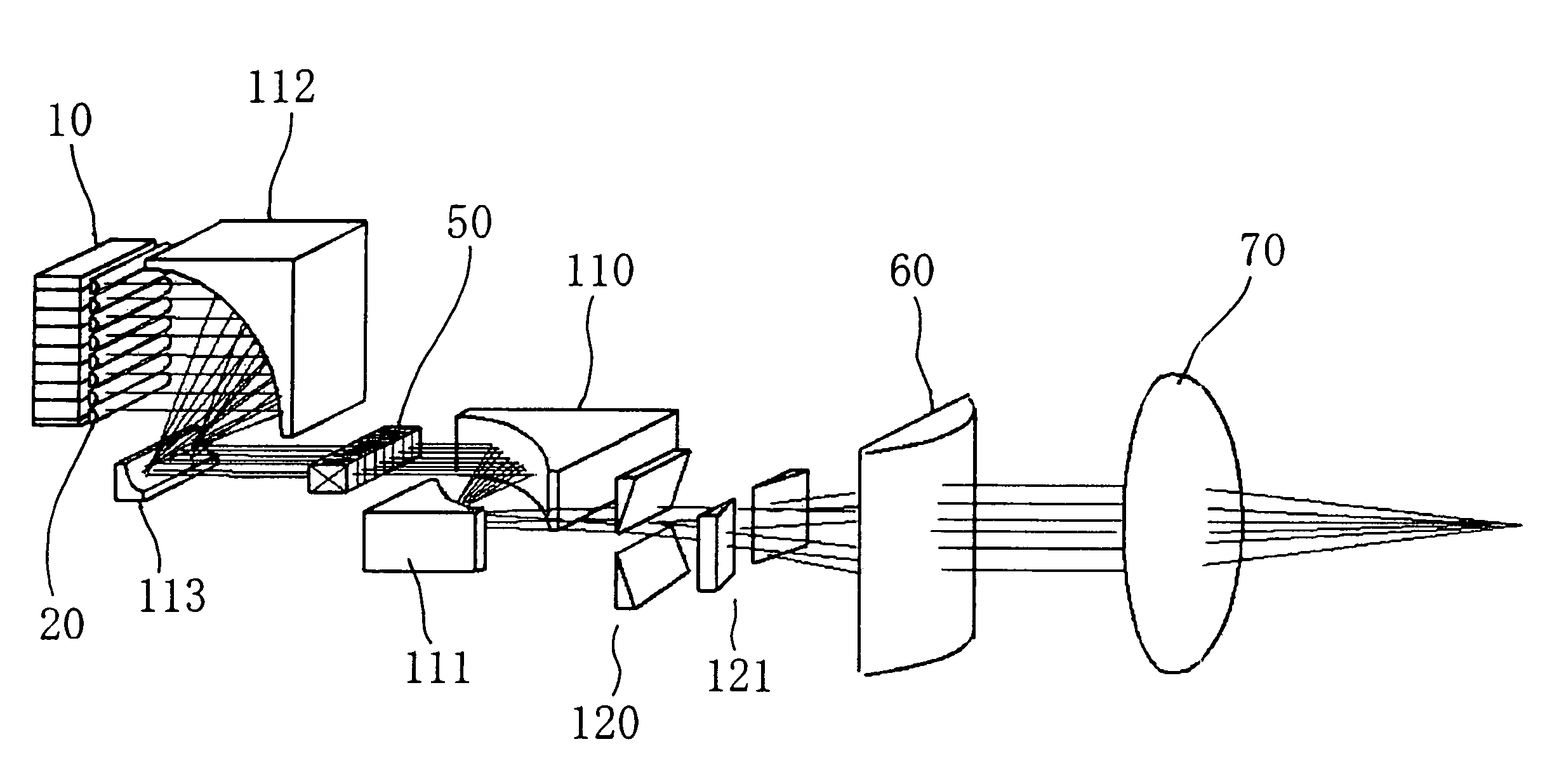
[0148]It has been described herein that a laser diode stack array is hard to focus since the divergence angles of the beams differ between the fast axis and the slow axis. According to an exemplary embodiment of the present invention, the technique may be used that rotates the beams by 90° to enable suitable collimation for each axis. Using such technique, it is possible to first collimate the large dispersion fast axis and later slowly and stably independently collimate the small dispersion slow axis.

[0149]Further, the laser diode stack array may form a planar light source comprised of a plurality of light sources having parallel optical axes arranged on the same plane.

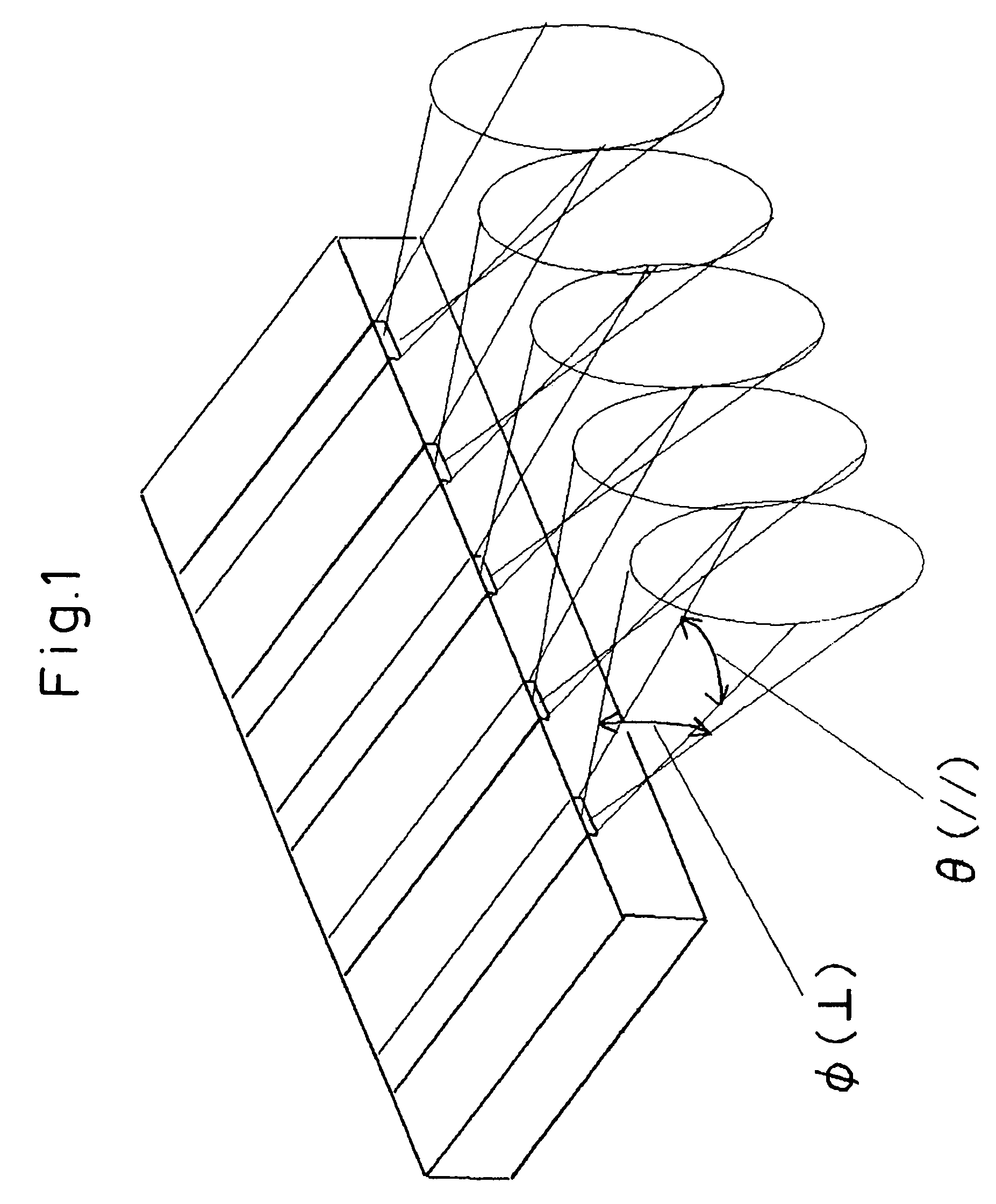
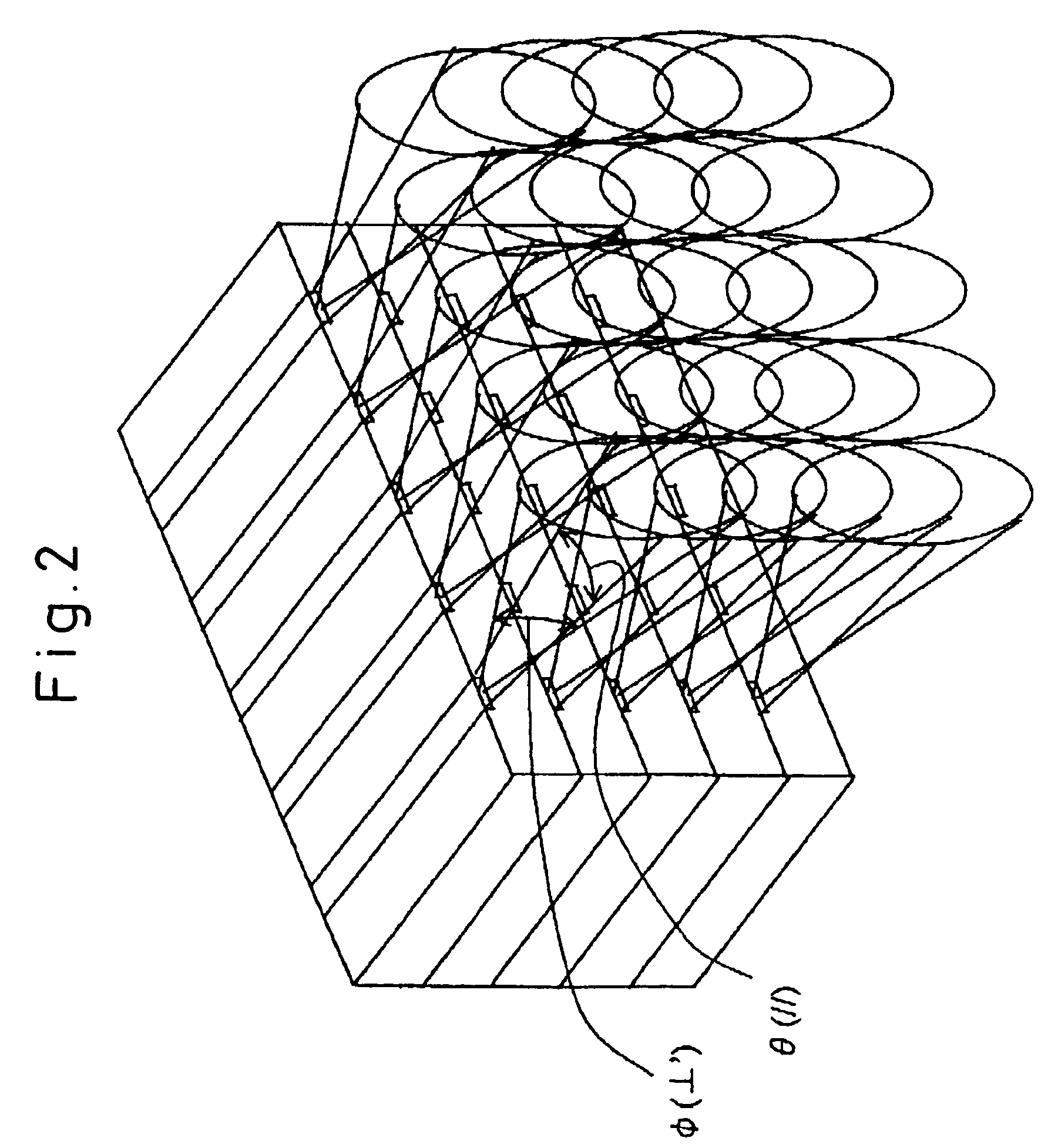
[0150]FIG. 3 shows the state of parallel beams entering a condensing lens having a focal length f. For simplification, the case of two parallel beams is shown. In such case, all beams are condensed at the focal point of the lens and a single image is obtained on the center axis.

[0151]On the other hand, when beams hav...


PUM


Abstract

A semiconductor laser device including a laser element stack array emitting a two-dimensional array shaped group of laser beams consisting of rows of laser beams arranged linearly in parallel in a broken line configuration and optical elements arranged in front of the array, receiving rows of laser beams bent and collimated in a direction substantially perpendicular to the orientation of the broken line configuration. Laser beams are emitted from emitters or groups of emitters and are rotated by right angles so as to convert the laser beams to a plurality of rows aligned in parallel in an approximate ladder rung configuration and the distance between center axes of the rows of laser beams is shortened to condense the laser beams by converting them to a group of laser beams emitted from a common object and thereby making all laser beams converge to a single image.

Description

CROSS-REFERENCE TO RELATED APPLICATION(S)[0001]This application claims priority under 35 U.S.C. § 119 from Japanese Patent Application No. 2003-194913 filed on Jul. 10, 2003, the entire disclosure of which is incorporated herein by reference.FIELD OF THE INVENTION[0002]The present invention relates to a beam converter capable of being used for a laser diode stack array and a laser device that is capable of using such beam converter. The present invention further relates to a semiconductor laser condenser capable of condensing semiconductor laser beams to a fine spot and a semiconductor laser pumped solid-state laser device configured to pump a beam of a solid-state laser element by semiconductor laser beams. A laser diode and a semiconductor laser is the same meanings here.BACKGROUND INFORMATION[0003]Linear arrays of semiconductor lasers comprised of active layer stripes of semiconductor lasers arranged one dimensionally and having a continuous wave (CW) output of about 50 W have be...

Claims


Application Information

Patent Timeline
Patent Type & Authority Patents(United States)
IPC IPC(8): H01S3/08G02B27/09H01S3/0941H01S5/00H01S5/40
CPCG02B27/0955H01S5/4031G02B19/0057G02B19/0028G02B19/0014H01S3/09415H01S5/005H01S5/0071H01S5/02284H01S5/4012H01S5/405H01S5/02251
Inventor IMAI, HIROFUMIHAMADA, NAOYAKIDO, MOTOISAKAI, TATSUHIKOSUGIHASHI, ATSUSHIHAMAMURA, HIDEYUKIYAMAGUCHI, SATOSHI
Owner NIPPON STEEL CORP
Why Eureka
Try Eureka