Semiconductor device with a nonvolatile semiconductor memory circuit and a plurality of IO blocks

a semiconductor memory circuit and nonvolatile technology, applied in semiconductor devices, digital storage, instruments, etc., can solve problems such as layout constraints, and achieve the effect of reducing the consideration of an arrangemen

Active Publication Date: 2007-07-03
PANASONIC SEMICON SOLUTIONS CO LTD
View PDF8 Cites 1 Cited by
  • Summary
  • Abstract
  • Description
  • Claims
  • Application Information

AI Technical Summary

Benefits of technology

[0007]An object of the present invention is to provide a semiconductor device which can solve a problem of a layout in consideration of a high voltage application to a CMOS device.
[0019]According to the present invention, by arranging the nonvolatile semiconductor memory circuit between the IO blocks, it will not be needed to supply a high voltage required for rewriting the CMOS device to an inside of the semiconductor device using a power supply interconnection while keeping an advantage on a circuit area that the upper interconnection can be freely utilized because physical processing of the device will not be needed due to replacing the conventional fuse element with the CMOS device. The internal interconnection and the semiconductor circuit may not therefore be influenced by the high voltage, thereby making it possible to reduce a consideration on an arrangement.

Problems solved by technology

However, since the CMOS device has required application of a high voltage for rewriting, it has been necessary to lay out a power supply interconnection so that the high voltage has been applied thereto from an external source outside the semiconductor device, and it has therefore been necessary to lay out the semiconductor devices so that interconnections other than that and semiconductor circuits adjacent to that interconnection path have not been influenced by the high voltage, that has resulted in constraints on the layout.

Method used


Image

  • Semiconductor device with a nonvolatile semiconductor memory circuit and a plurality of IO blocks
  • Semiconductor device with a nonvolatile semiconductor memory circuit and a plurality of IO blocks
  • Semiconductor device with a nonvolatile semiconductor memory circuit and a plurality of IO blocks

Examples


Embodiment Construction

[0022]Hereafter, referring to the drawings, description will be made of an embodiment of the present invention.

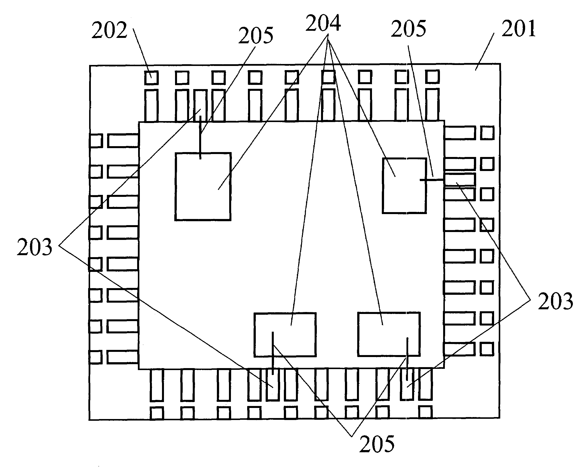
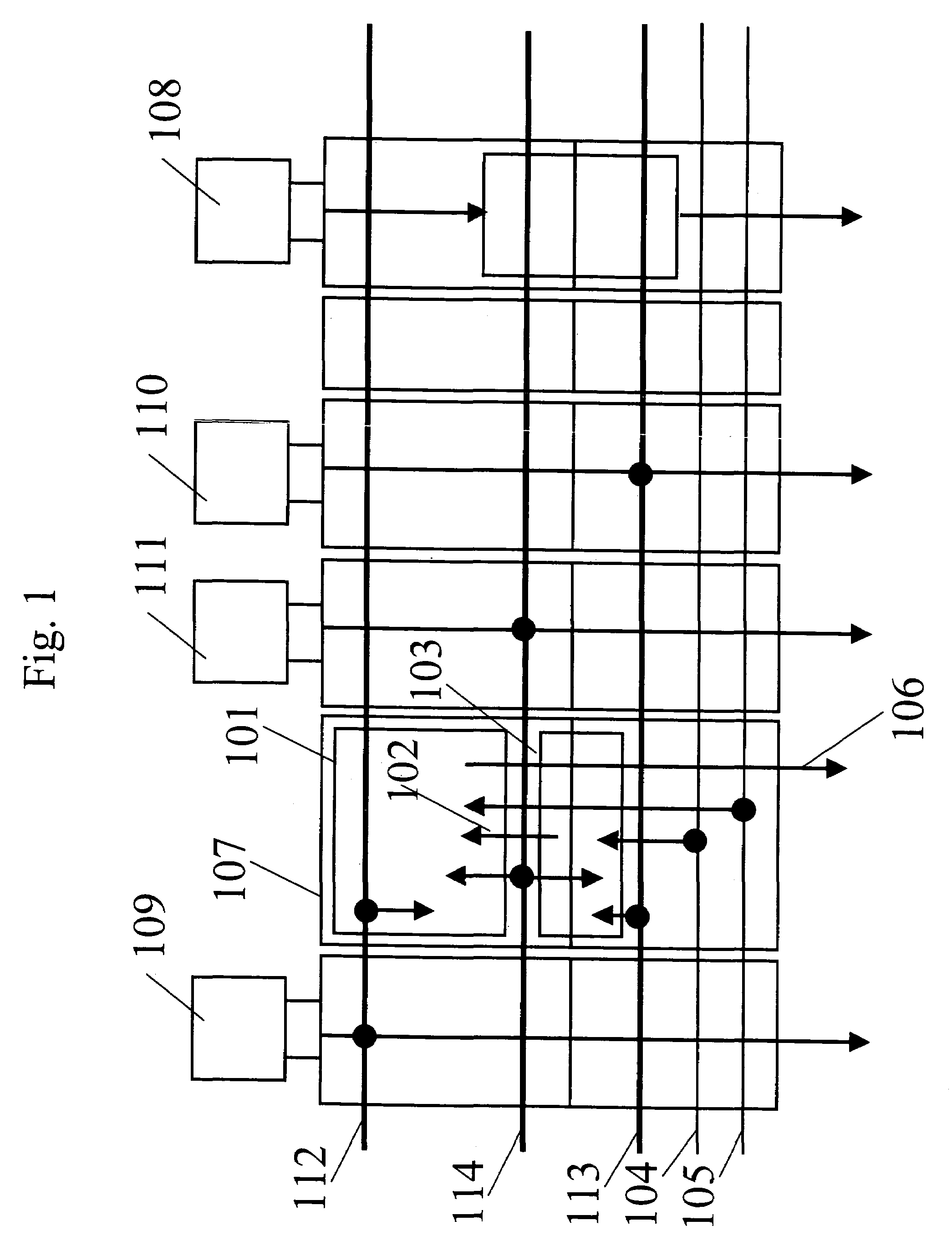
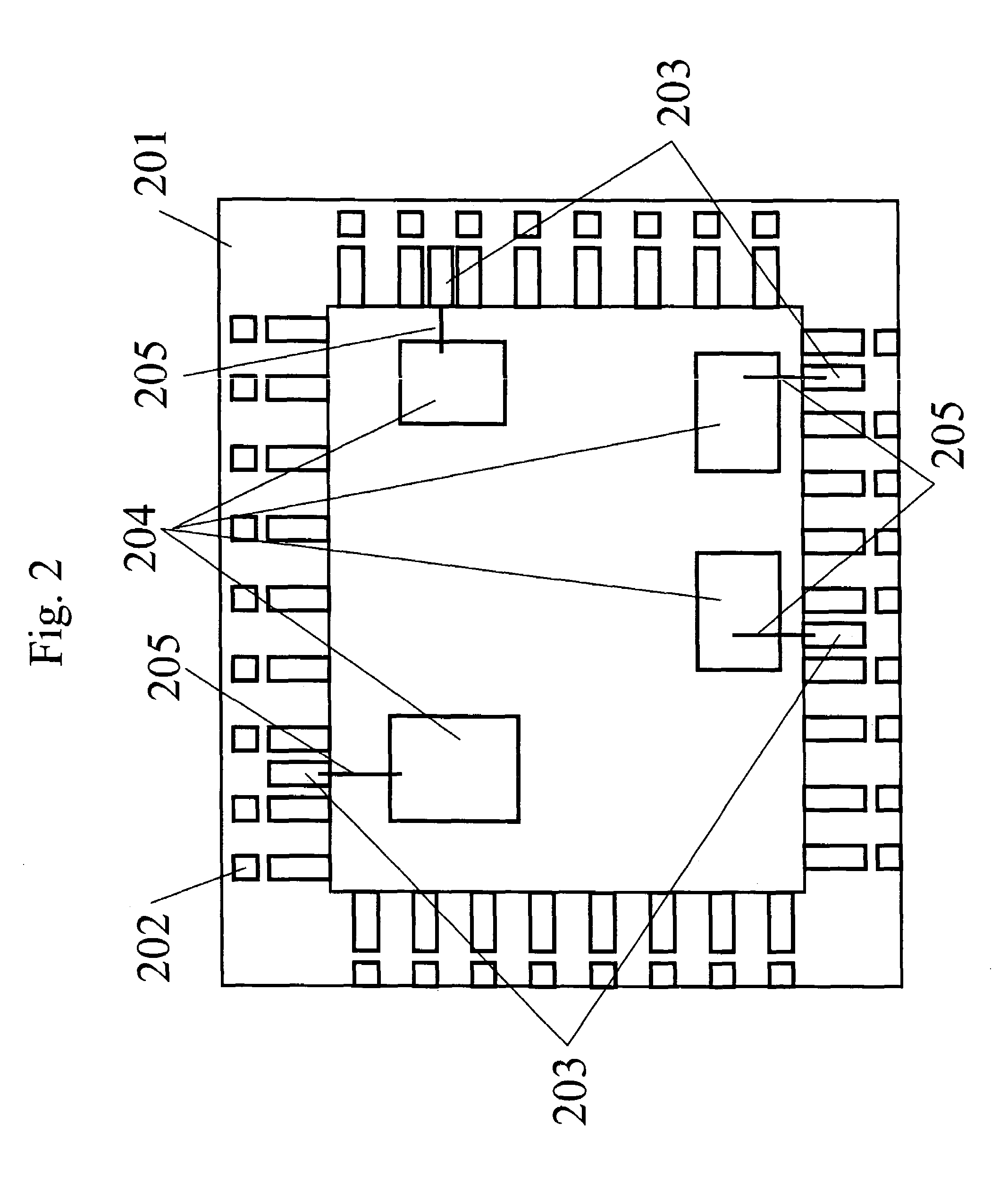
[0023]FIG. 1 and FIG. 2 show a block diagram of a semiconductor device in accordance with the embodiment of the present invention. In FIG. 1, reference numeral 101 represents a nonvolatile memory device constituted of an electrically readable and writable CMOS device; reference numeral 102, a set of control signals for controlling a write to the nonvolatile memory device 101; reference numeral 103, a control circuit for producing the set of control signals; reference numeral 104, a set of address signals supplied to the control circuit 103; reference numeral 105, a data line for supplying data written to the nonvolatile memory device 101 synchronizing with the set of control signals; reference numeral 106, a data line for producing data written to the nonvolatile memory device 101; reference numeral 107, a nonvolatile semiconductor memory circuit; reference numeral 108, an ...


PUM


Abstract

Only by replacing a conventional fuse element used for a redundant repair of a memory with a CMOS device, since physical processing is not required, there is an advantage on a circuit area in which the upper interconnection can be utilized. However, on a design of a semiconductor device, since the CMOS device requires application of a high voltage for rewriting, there is a problem of being subjected constraint of an arrangement of an interconnection or a semiconductor circuit. For that reason, by arranging the nonvolatile semiconductor memory circuit provided with the nonvolatile memory device which is constituted of a CMOS device between the IO blocks arranged at the periphery of the chip, physical processing due to replacing the conventional fuse element with the CMOS device will not be needed, so that while keeping an advantage on a circuit area that the upper interconnection can be utilized, the problem of the arrangement in consideration of high voltage application can be resolved.

Description

BACKGROUND OF THE INVENTION[0001]1. Field of the Invention[0002]The present invention relates to a semiconductor device.[0003]2. Description of the Prior Art[0004]In a field of a semiconductor integrated circuit device in recent years, high integration owing to progress of a microfabrication technology has been increasingly accelerated in conjunction with a competition between semiconductor makers. At the same time, cost reduction is also an imperative for these semiconductor makers, and not only in a field of a general-purpose memory, such as general-purpose DRAM and synchronous DRAM, but also in a field of a system LSI where a microprocessor, ASIC, custom logic or the like and a memory are built into one chip, in order to satisfy above imperative, a method of improving a yield by employing a redundant repair technology using a fuse in which a faulty memory cell generated in a manufacturing step is replaced with a spare memory cell has become important. Meanwhile, as an application...

Claims


Application Information

Patent Timeline
Patent Type & Authority Patents(United States)
IPC IPC(8): G11C16/04G11C7/00H01L21/822G11C16/02G11C29/00H01L21/82H01L27/04
CPCG11C29/80
Inventor NAKAI, NOBUYUKI
Owner PANASONIC SEMICON SOLUTIONS CO LTD
Why Eureka
Try Eureka