Method for fabricating semiconductor devices

a technology of nitride and light-emitting devices, which is applied in the direction of semiconductor devices, basic electric elements, electrical equipment, etc., can solve the problems of increasing series resistance, increasing device size, and reducing yield, so as to prevent a reduction in yield

Inactive Publication Date: 2007-07-17
PANASONIC CORP
View PDF8 Cites 19 Cited by
  • Summary
  • Abstract
  • Description
  • Claims
  • Application Information

AI Technical Summary

Benefits of technology

[0024]In view of the foregoing, it is therefore an object of the present invention to provide a method for fabricating semiconductor devices which prevents a reduction in yield and allows a plurality of semiconductor devices to be separated from each other.

Problems solved by technology

This causes the problem of increased series resistance due to an elongated current path and the problem of increased device size.
First, in the method for fabricating semiconductor devices according to the first conventional embodiment, the function of the thin-film GaN layer 102 as a holding member is degraded if the bonding strength of the Cu plate 105 is extremely low. Consequently, there are cases where the GaN layer 102 is naturally split in the step of performing cleavage. Since such naturally split chips mostly have rough and uneven surfaces, they cannot be used as devices, which causes a reduction in yield. Conversely, if the bonding strength of the Cu plate 105 is high, there are cases where the Cu plate 105 is not separated even when the thin-film GaN layer 102 is separated by cleavage, which also causes a reduction in yield. Thus, the method for fabricating semiconductor devices according to the first conventional embodiment requires strict control of the bonding strength of the Cu plate.
If the film thickness of the Au plate 204 is large, however, it is difficult during patterning to recognize a layer serving as an underlie for the Au plate 204 so that mask alignment becomes difficult, which causes a reduction in yield.
Thus, it is also difficult to achieve a high yield even in accordance with the method for fabricating semiconductor devices according to the second embodiment.

Method used


Image

  • Method for fabricating semiconductor devices
  • Method for fabricating semiconductor devices
  • Method for fabricating semiconductor devices

Examples


embodiment 1

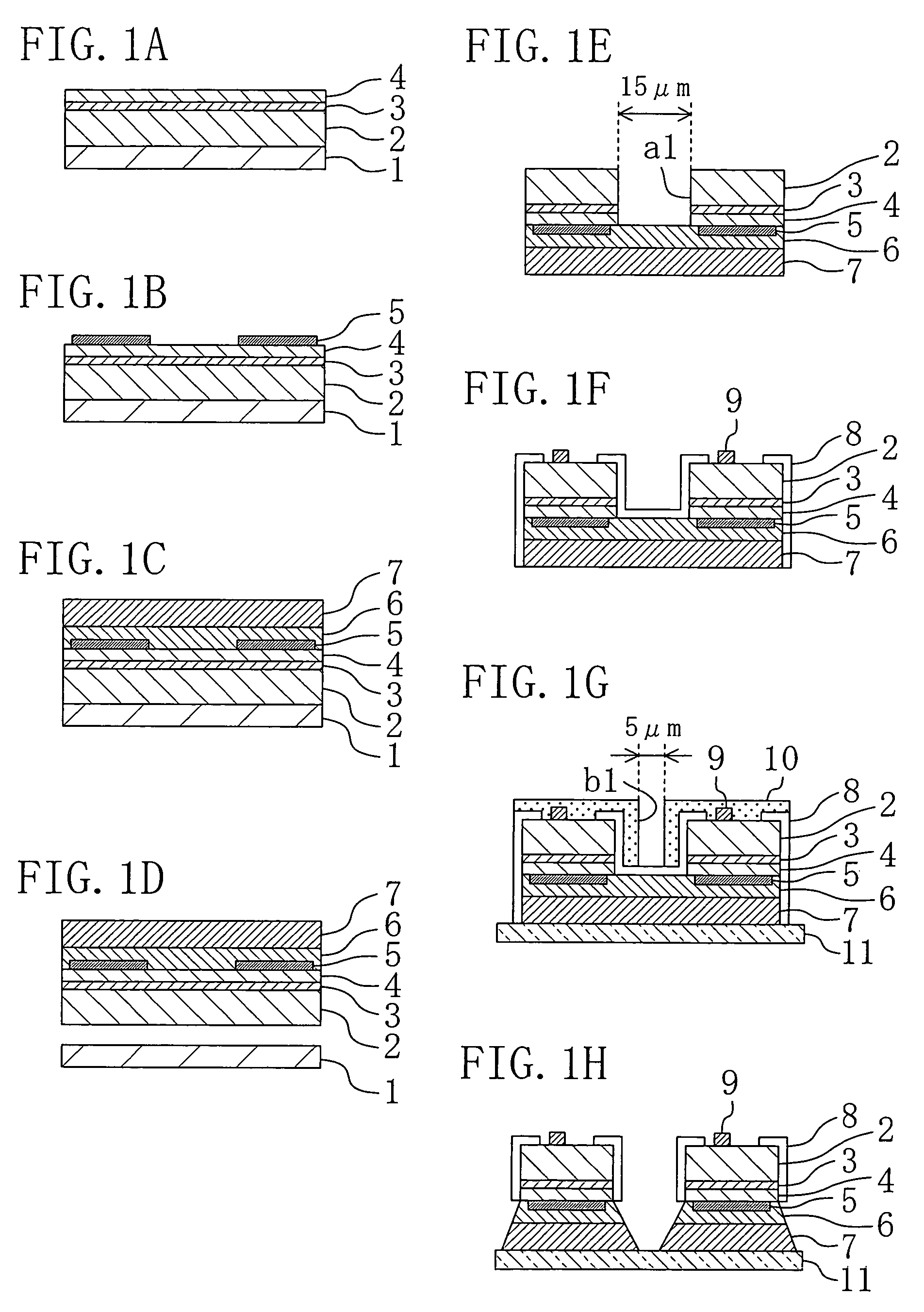
[0057]Referring to FIGS. 1A to 1H, a method for fabricating semiconductor devices according to a first embodiment of the present invention will be described by using, as a specific example, a method for fabricating blue surface emitting devices each composed of a nitride semiconductor.

[0058]As a system for growing a GaN layer, a MOVPE (metal organic vapor phase epitaxy) system is used. As a Ga raw material, trimethylgallium is used, while NH3 is used as an N raw material. As an Si raw material serving as a donor impurity, SiH4 is used, while H2 is used as a carrier gas.

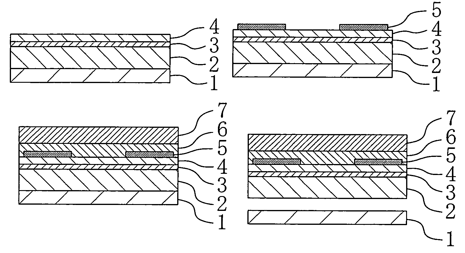
[0059]First, as shown in FIG. 1A, a low-temperature buffer layer (not shown) is formed on a 2-inch (0001) sapphire substrate 1. Then, an n-type GaN layer 2 is grown on the low-temperature buffer layer to have a film thickness of 4 μm. In this case, a growth temperature for the GaN layer 2 is 1030° C. Subsequently, the carrier gas is switched to N2 and the growth temperature is reduced to 800° C. so that an active laye...

embodiment 2

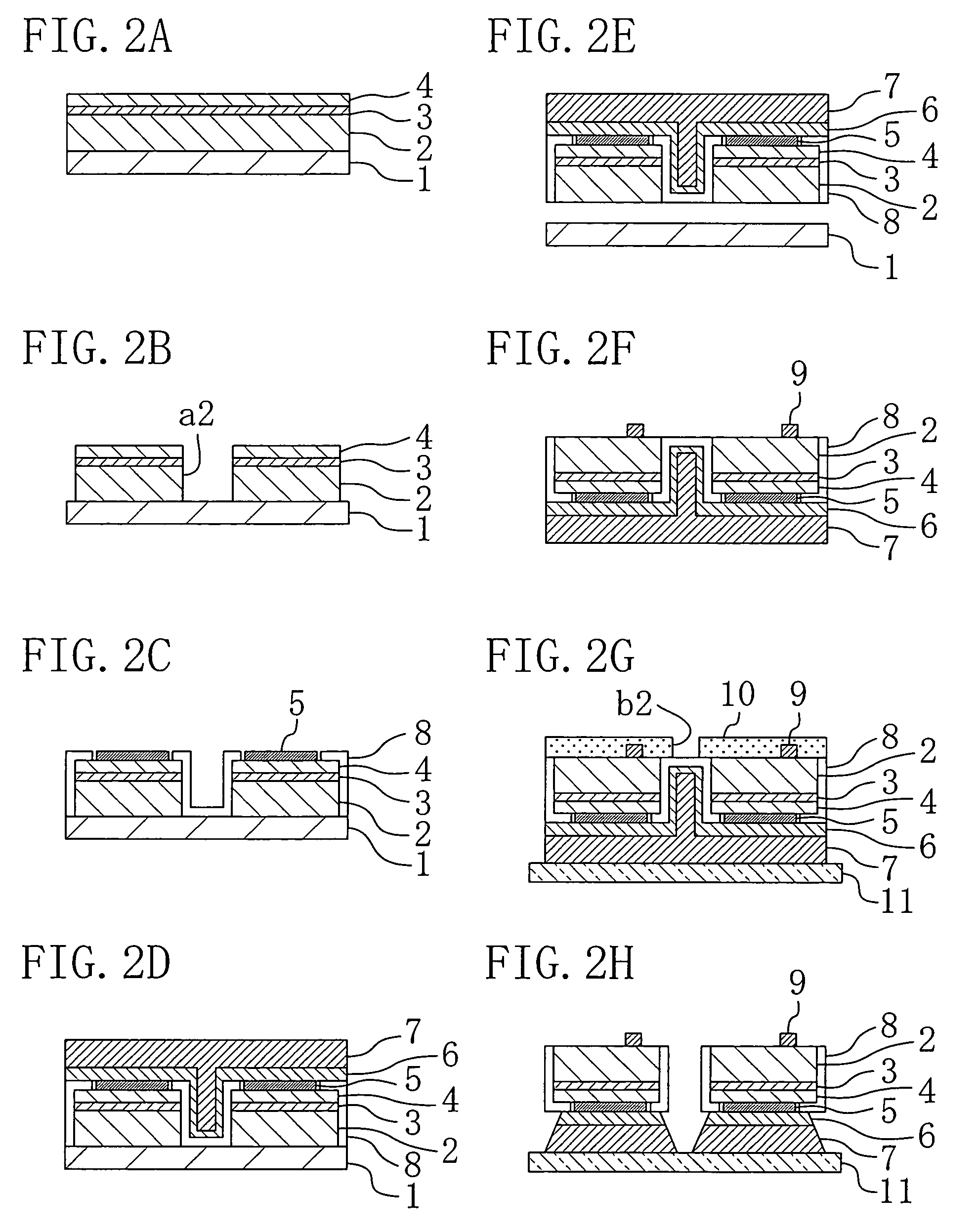
[0071]Referring to FIGS. 2A to 2H, a method for fabricating semiconductor devices according to a second embodiment of the present invention will be described by using, as a specific example, a method for fabricating blue surface emitting devices each composed of a nitride semiconductor. In FIGS. 2A to 2H, the components corresponding to those shown in the drawings described above are designated by the same reference numerals.

[0072]First, as shown in FIG. 2A, the steps of successively depositing the n-type GaN layer 2, the active layer 3, and the p-type GaN layer 4 on the sapphire substrate 1 and performing annealing are performed in the same manner as in the first embodiment that has been described with reference to FIG. 1A.

[0073]Next, as shown in FIG. 2B, a mask is formed on the p-type GaN layer 4 and then the portions of the nitride semiconductor layers which are present in the chip isolation region of each of the n-type GaN layer 2, the active layer 3, and the p-type GaN layer 4 ...

embodiment 3

[0084]Referring to FIGS. 3A to 3I, a method for fabricating semiconductor devices according to a third embodiment of the present invention will be described by using, as a specific example, a method for fabricating blue surface emitting devices each composed of a nitride semiconductor. In FIGS. 3A to 3I, the components corresponding to those shown in the drawings described above are designated by the same reference numerals.

[0085]As a system for growing a GaN layer, a MOVPE (metal organic vapor phase epitaxy) system is used. As a Ga raw material, trimethylgallium is used. As an Al raw material, trimethylaluminum is used, while NH3 is used as an N raw material. As an Si raw material serving as a donor impurity, SiH4 is used, while H2 is used as a carrier gas. As an Mg raw material serving as an acceptor impurity, cyclopentadienylmagnesium is used.

[0086]First, as shown in FIG. 3A, the low-temperature buffer layer (not shown) is formed on the 2-inch (0001) sapphire substrate 1. Then, a...


PUM

PropertyMeasurementUnit
thicknessaaaaaaaaaa
thicknessaaaaaaaaaa
thicknessaaaaaaaaaa

Abstract

A method for fabricating semiconductor devices forms a semiconductor layer containing a positive layer on a mother substrate and then forms a metal layer on the semiconductor layer. After forming the metal layer, the method separates the mother substrate from the semiconductor layer and then removes a desired region of the metal layer from the exposed surface of the semiconductor layer from which the mother substrate has been separated to form a plurality of mutually separated semiconductor devices each containing the semiconductor layer.

Description

BACKGROUND OF THE INVENTION[0001]The present invention relates to a method for fabricating nitride semiconductor light-emitting devices which emit light in blue-to-ultraviolet regions.[0002]Currently, light-emitting diodes each using a group III nitride have been widely commercialized for various types of displays, large-scale displays, signal lights, or the like. In addition, white LEDs each composed of a combination of a GaN LED and a fluorescent material have also been commercialized and expected to replace lighting devices used at present provided that the light emission efficiencies thereof will be improved in future.[0003]In general, a group III nitride semiconductor (hereinafter simply referred to as a nitride semiconductor) composed of GaN or the like has been formed on a sapphire substrate as mainstream practice. However, since the sapphire substrate has no conductivity, it is necessary to form a p-type electrode and an n-type electrode on the same plane in a GaN growth lay...

Claims


Application Information

Patent Timeline
Patent Type & Authority Patents(United States)
IPC IPC(8): H01L21/00H01L21/20H01L33/00
CPCH01L21/2007H01L33/0079H01L33/0093H01L2224/83
Inventor TAMURA, SATOSHIUEDA, TETSUZO
Owner PANASONIC CORP
Why Eureka
Try Eureka