Method of manufacturing semiconductor devices

a semiconductor and manufacturing method technology, applied in the field of semiconductor devices, can solve the problems of inability to apply constitution to the pixel tft, increase of off current, etc., and achieve the effect of suppressing preventing an increase in off current, and preventing deterioration of on curren

Inactive Publication Date: 2007-07-17
SEMICON ENERGY LAB CO LTD
View PDF45 Cites 16 Cited by
  • Summary
  • Abstract
  • Description
  • Claims
  • Application Information

AI Technical Summary

Benefits of technology

[0019]For a pixel area of the liquid crystal display and drive circuits made basically of CMOS circuits arranged around the pixel area, it is a third object of the invention to provide a constitution in which the LDD region of at least an n-channel TFT overlaps a gate electrode and which can prevent an increase in the OFF current, and to provide a method of manufacturing the constitution.
[0022]Hence, the constitution shown in FIGS. 17(A-1), (A-2), and (A-3) cannot simultaneously satisfy both of the ON region characteristic and the OFF region characteristic required by the pixel area, within the reliability requirement. It has been found, however, that the use of the constitution of FIG. 17(A-4) can prevent deterioration of the ON current and suppress an increase in the OFF current. This can be achieved by dividing the LDD region into a region that overlaps the gate electrode and a region that does not. The LDD region overlapping the gate electrode has a function of suppressing a hot carrier injection phenomenon and the LDD region not overlapping the gate electrode has a function of preventing an increase in the OFF current.

Problems solved by technology

The GOLD constitution has a problem that when a high gate voltage is applied thereto at the OFF characteristic, the OFF current is increased.
In this constitution, the ON current and the OFF current are both high and the degradation due to the bias stress is large, so that this constitution cannot be applied to the pixel TFT.

Method used


Image

  • Method of manufacturing semiconductor devices
  • Method of manufacturing semiconductor devices
  • Method of manufacturing semiconductor devices

Examples


example 1

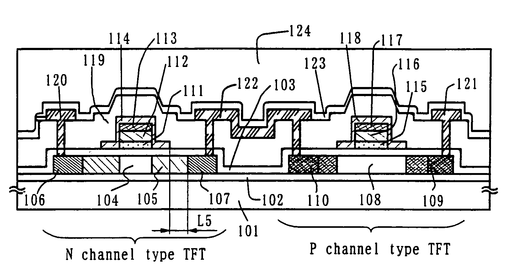
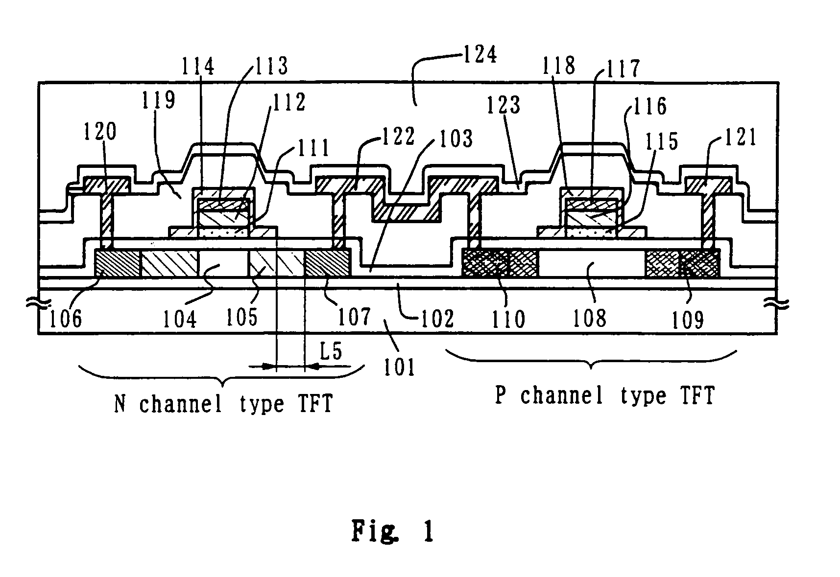
[0089]This example describes a constitution of this invention, a method of manufacturing simultaneously a pixel area and CMOS circuits that are basic configuration of driving circuits provided around the pixel area.

[0090]In FIG. 2, a substrate 201 is an alkali-free glass substrate, represented, for example, by 1737 glass substrate of Corning make. The surface of the substrate 201 where the TFT is to be formed is deposited with a base film 202 made mainly of silicon oxide to a thickness of 200 nm. The base film 202 may use a silicon nitride film or silicon oxynitride film.

[0091]The base film 202 may be formed in a single layer of the material above or in two or more layers. In either case, it is formed to a thickness of about 100 to 300 nm. For example, the base film 202 may be formed by a plasma CVD method as a two-layer constitution, in which a first silicon oxynitride film is formed from SiH4, NH3 and N2O to a thickness of 10 to 100 nm and a second silicon oxynitride film from SiH...

example 2

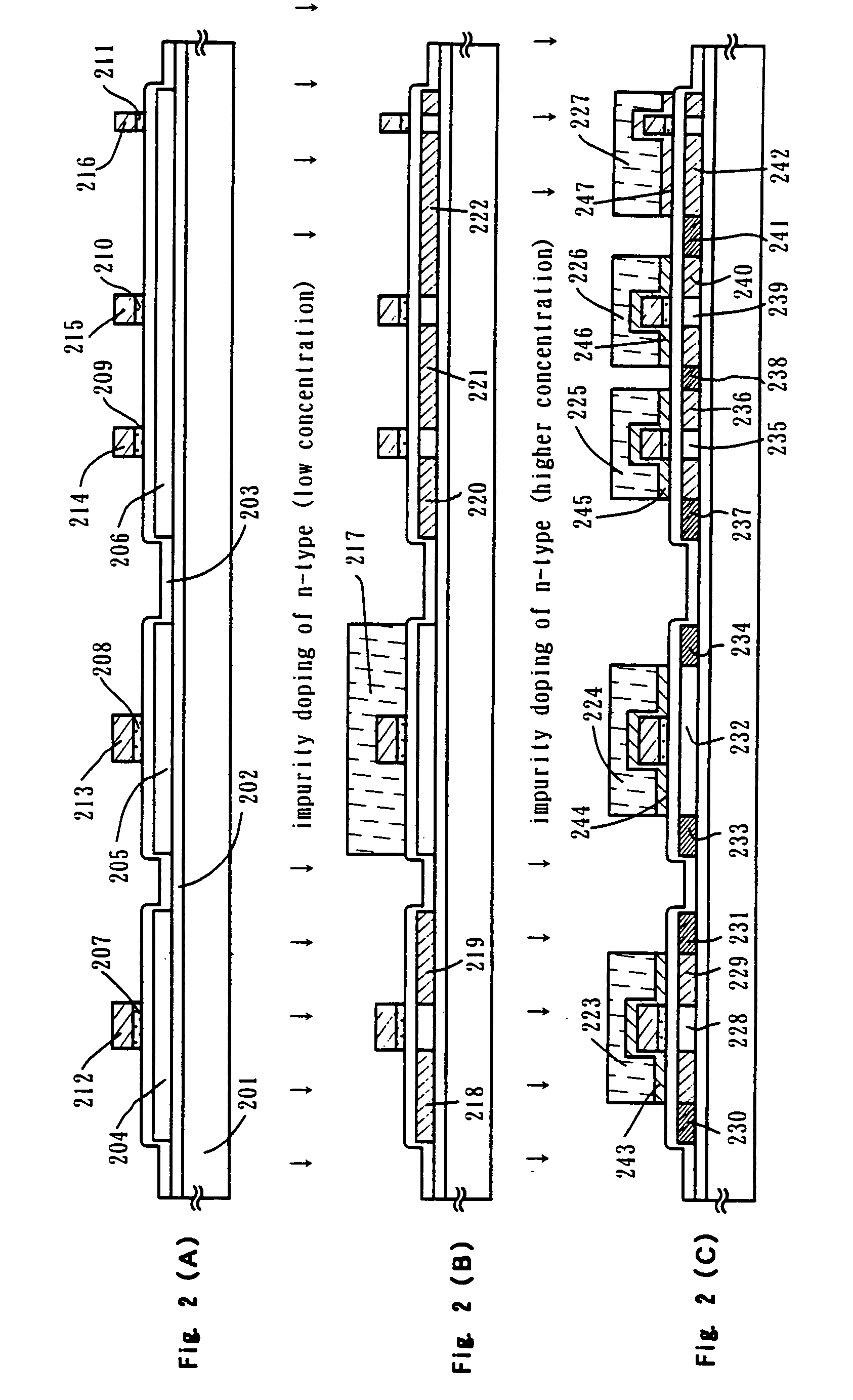
[0117]This example shows an example case where, after the state shown in FIG. 2(C) has been obtained by the same process as in the example 1, a part of the second conductive layer is removed by other method to form a region where the first impurity region overlaps the second conductive layer and a region where it does not.

[0118]First, as shown in FIG. 2(C), the resist masks 223, 224, 225, 226, 227 used in the process of patterning the second conductive layer are used as is to etch back a part of the second gate electrode by a length L5 as shown in FIG. 4(A).

[0119]This process was performed by dry etching. Depending on the material of the second conductive layer, a fluorine-based gas is basically used to achieve an isotropic etch and thereby remove those parts of the second conductive layer beneath the resist masks. The etching gas, for example, is a CF4 gas for Ta, a CF4 or CCl4 gas for Ti, and an SF6 or NF3 for Mo.

[0120]Then, as shown in FIG. 4(B), the second conductive layer is re...

example 3

[0122]This example describes a process of manufacturing an active matrix liquid crystal display from an active matrix substrate formed in the example 1 or example 2.

[0123]In the active matrix substrate as shown in FIG. 3(C) or FIG. 4(C), contact holes are formed in the second interlayer insulating film 270 to reach the drain line 268, and then a pixel electrode 271 is formed. The pixel electrode 271 uses a transparent conductive film for a transmission type liquid crystal display and a metal film for a reflection type liquid crystal display. Here, in order to fabricate a transmission type liquid crystal display, an indium-tin oxide (ITO) film is sputtered to a thickness of 100 nm to form the pixel electrode 271.

[0124]After the state of FIG. 5(A) is obtained, an alignment film 272 is formed over the second interlayer insulating film 270 and the pixel electrode 271. Generally, the alignment film for the liquid crystal display element often uses a polyimide resin. A counter substrate 2...


PUM

PropertyMeasurementUnit
gate voltageaaaaaaaaaa
distanceaaaaaaaaaa
resistivityaaaaaaaaaa

Abstract

Subjected to obtain a crystalline TFT which simultaneously prevents increase of OFF current and deterioration of ON current. A gate electrode of a crystalline TFT is comprised of a first gate electrode and a second gate electrode formed in contact with the first gate electrode and a gate insulating film. LDD region is formed by using the first gate electrode as a mask, and a source region and a drain region are formed by using the second gate electrode as a mask. By removing a portion of the second gate electrode, a structure in which a region where LDD region and the second gate electrode overlap with a gate insulating film interposed therebetween, and a region where LDD region and the second gate electrode do not overlap, is obtained.

Description

[0001]This application is a divisional of U.S. application Ser. No. 10 / 292,830, filed on Nov. 12, 2002 now U.S. Pat. No. 6,815,273 which is a divisional of U.S. application Ser. No. 09 / 441,025, filed on Nov. 16, 1999 now U.S. Pat. No. 6,518,594 issued Feb. 11, 2003.BACKGROUND OF THE INVENTION[0002]1. Field of the Invention[0003]The present invention relates to a semiconductor device having a circuit comprising thin-film transistors on a substrate with an insulating surface and to a method of manufacture thereof. More specifically, the invention relates to a constitution of an electrooptical device represented by a liquid crystal display and of an electronic apparatus mounting the electrooptical device. In this specification, the semiconductor device generally denotes devices that function by utilizing semiconductor characteristics and includes the electrooptical devices and the electronic apparatus mounting the electrooptical devices.[0004]2. Related Art[0005]The thin-film transisto...

Claims


Application Information

Patent Timeline
Patent Type & Authority Patents(United States)
IPC IPC(8): H01L29/04G02B27/00G02B27/01G02F1/1362H01L21/336H01L21/77H01L21/84H01L29/423H01L29/786
CPCG02B27/017H01L29/42384H01L29/78621H01L29/78627H01L27/124H01L29/66757G02B2027/0138G02F1/13454H01L27/3244H01L29/78624H10K59/12
Inventor NAKAJIMA, SETSUOOHTANI, HISASHIYAMAZAKI, SHUNPEI
Owner SEMICON ENERGY LAB CO LTD
Why Eureka
Try Eureka