Memory device with different termination units for different signal frequencies

a memory device and signal frequency technology, applied in the field of memory devices with different termination units for different signal frequencies, can solve the problems of power consumption disadvantageously increased, high power consumption, and signal distortion on data transfer lines, and achieve the effects of less signal distortion, reduced power consumption, and reduced power consumption

Inactive Publication Date: 2007-08-07
SAMSUNG ELECTRONICS CO LTD
View PDF16 Cites 3 Cited by
  • Summary
  • Abstract
  • Description
  • Claims
  • Application Information

AI Technical Summary

Benefits of technology

[0013]Accordingly, in a general aspect of the present invention, both signal distortion and power consumption are minimized by using termination units of different types for input signals of different frequencies for the semiconductor memory device.
[0023]In this manner, the memory device and system of the present invention use different termination units of different types for different frequencies of the input signals. When an input signal has a higher frequency, the termination unit of the push-pull type is used for providing less signal distortion for such a higher frequency input signal. On the other hand, when the input signal has a lower frequency, the termination unit of the open-drain type is used for lower power consumption since signal distortion is already less for input signals of lower frequency. Thus, both signal distortion and power consumption are minimized for the memory device and system according to embodiments of the present invention.

Problems solved by technology

However, when the aforementioned interface techniques are used for a memory device having an operating frequency of 400 MHz or more, signal distortion tends to occur on the data transfer lines.
On the other hand, the push-pull type termination unit 21 of FIG. 1B is particularly advantageous for memory devices operating with higher frequencies because signal distortion is smaller, but disadvantageously has higher power consumption.
However, semiconductor memory devices of the prior art disadvantageously use termination units of the same type for all the input signal lines and the data input / output signal lines.
When termination units of the push-pull type are used for all the signal lines of a semiconductor memory device for lower signal distortion, power consumption is disadvantageously increased.
On the contrary, when termination units of the open-drain type are used for all the signal lines for lower power consumption, signal distortion is disadvantageously increased.

Method used


Image

  • Memory device with different termination units for different signal frequencies
  • Memory device with different termination units for different signal frequencies
  • Memory device with different termination units for different signal frequencies

Examples


Embodiment Construction

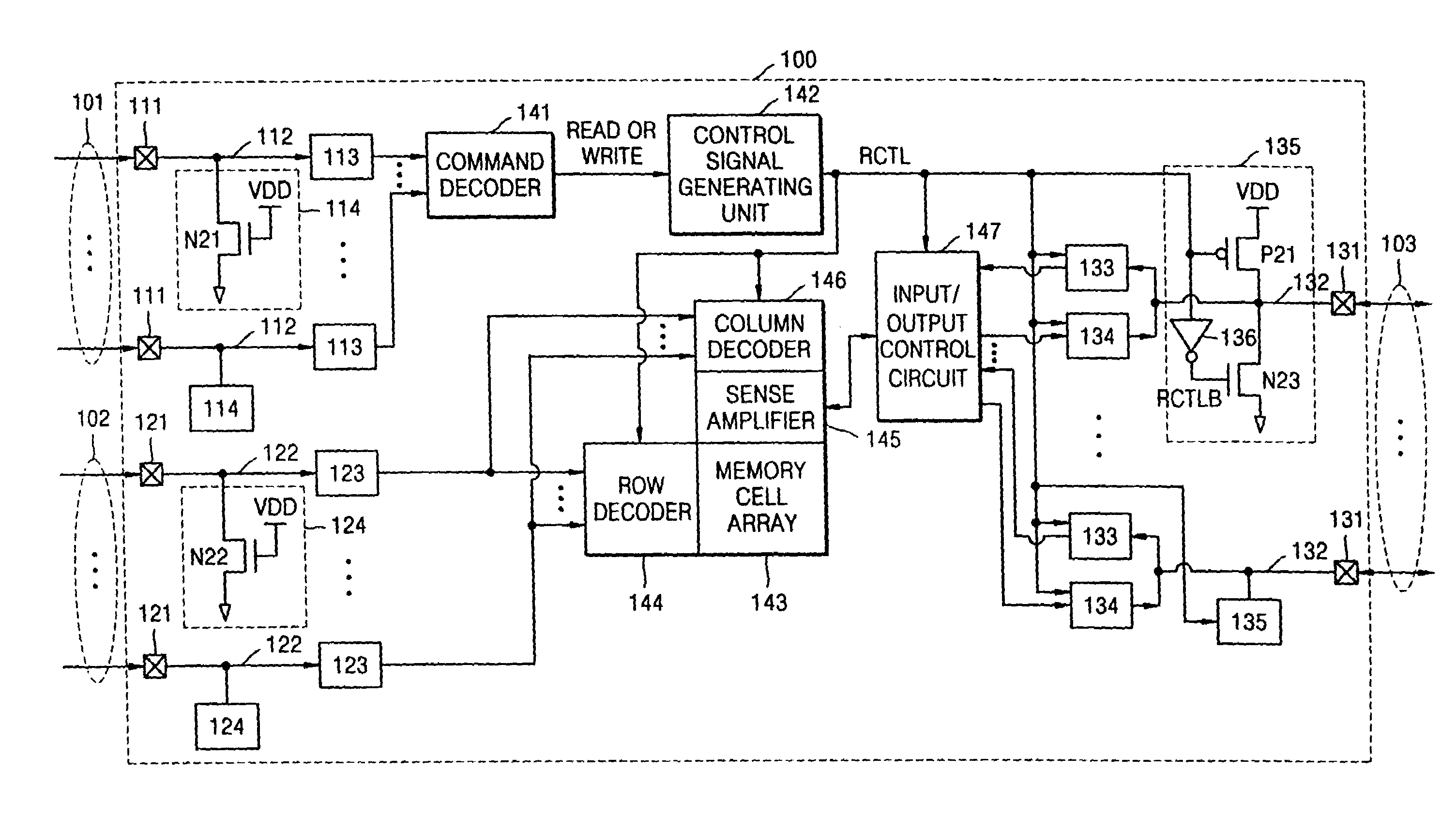
[0033]FIG. 3 is a diagram illustrating a semiconductor memory device 100 according to an embodiment of the present invention. The semiconductor memory device 100 includes components fabricated as an integrated circuit on a semiconductor substrate such as a silicon substrate in one example embodiment of the present invention. For example, the dashed lines inFIG. 3 may out-line the semiconductor substrate having the components of the memory device 100 fabricated therein.

[0034]Referring to FIG. 3, the semiconductor memory device 100 comprises control pins 101, address pins 102, and data pins 103. Each of the control pins 101 is coupled to a respective one of a first set of input / output pads 111, and each of the data pins 103 is coupled to a respective one of a second set of input / output pads 131. Each of the address pins 102 is coupled to a respective one of a third set of input / output pads 121.

[0035]The semiconductor memory device 100 further comprises external control signal input bu...


PUM


Abstract

A memory device includes a first termination unit coupled to a first pin for receiving a first signal having a first frequency component. The memory device also includes a second termination unit coupled to a second pin for receiving a second signal having a second frequency component higher than the first frequency component. The first termination unit is a different type from the second termination unit that provides less signal distortion than the first termination unit. For example, the first termination unit is of an open-drain type that has less power consumption, and the second termination unit is of a push-pull type that has less signal distortion.

Description

[0001]This application claims priority to Korean Patent Application No. 2004-009940, filed on Feb. 16, 2004 in the Korean Intellectual Property Office, the disclosure of which is incorporated herein in its entirety by reference.BACKGROUND OF THE INVENTION[0002]1. Field of the Invention[0003]The present invention relates generally to semiconductor memory devices, and more particularly, to termination units for such memory devices.[0004]2. Description of the Related Art[0005]With increase in data transfer rate between a semiconductor memory device and a memory controller, interface techniques for reducing distortion of transferred data and for more accurate transfer of data are desired. Examples of such interface techniques include a low voltage transistor-transistor logic (LVTTL) interface technique and a stub-series terminated logic (SSTL) interface technique.[0006]For the LVTTL interface technique, a synchronous dynamic random access memory (SDRAM) and a memory controller are direc...

Claims


Application Information

Patent Timeline
Patent Type & Authority Patents(United States)
IPC IPC(8): G11C7/00H03K17/16G06F12/00G06F13/16G11C7/10G11C11/409
CPCG11C7/1048G11C7/1078G11C7/1084G11C2207/105A23B7/02A23B4/031F26B3/02A23V2300/10
Inventor LEE, JUNG-JOON
Owner SAMSUNG ELECTRONICS CO LTD
Why Eureka
Try Eureka