Integrated passive devices

a passive device and integrated technology, applied in the direction of capacitors, semiconductor/solid-state device details, inductances, etc., can solve the problems of no value as active device substrates, more than adequate for producing large substrates, and polysilicon as a substrate material has been largely overlooked, so as to achieve high resistivity and cost-effective

Inactive Publication Date: 2007-08-21
SYCHIP
View PDF3 Cites 22 Cited by
  • Summary
  • Abstract
  • Description
  • Claims
  • Application Information

AI Technical Summary

Benefits of technology

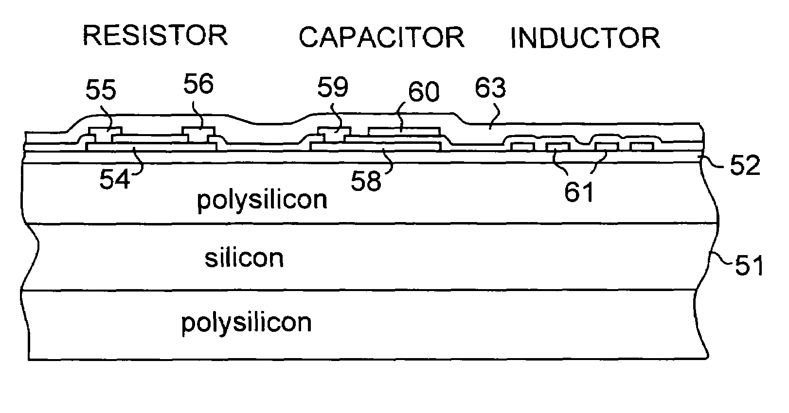
[0007]We have discovered a new IPD substrate material with properties that are compatible with highly integrated thin film structures. The new substrate material is polysilicon. Polysilicon layers have been used widely in integrated circuit technology for many years, and the technology of polysilicon, both in terms of properties and thin film deposition techniques, is well known and well developed. However, polysilicon as a substrate material has been largely overlooked until now. It is known that polysilicon can be made with relatively high resistivity, and that a variety of components and devices can be built on polysilicon layers acting as insulating layers. However, our approach melds several known elements in integrated circuit fabrication technology to produce a practical, cost effective, high resistivity, polysilicon substrate as the basic building block for highly integrated IPD circuits. In this approach the polysilicon substrate is self-supporting and can be processed, handled, and packaged. In a preferred embodiment, the polysilicon substrate is produced using a single crystal silicon wafer as a starting material. The polysilicon substrate is made by depositing a thick substrate layer on the silicon wafer, forming a plurality of IPDs at the wafer level, and removing the silicon wafer. Prior art technologies, for example gated diode switches (GDXs), have used polysilicon as “handles” to facilitate processing and handling of single crystal layers or tubs. However, the use of single crystal silicon in this manner is believed to be novel. It is also unobvious, since conventional thought would reject using an expensive material—single crystal silicon—as a sacrificial element in a process. However, we have overcome that thinking by using large silicon wafers that are manufacturing rejects, and are thus of no value as active device substrates. However, they are more than adequate for producing large substrates of polysilicon.

Problems solved by technology

However, polysilicon as a substrate material has been largely overlooked until now.
It is also unobvious, since conventional thought would reject using an expensive material—single crystal silicon—as a sacrificial element in a process.
However, we have overcome that thinking by using large silicon wafers that are manufacturing rejects, and are thus of no value as active device substrates.
However, they are more than adequate for producing large substrates of polysilicon.

Method used


Image

  • Integrated passive devices
  • Integrated passive devices
  • Integrated passive devices

Examples


Embodiment Construction

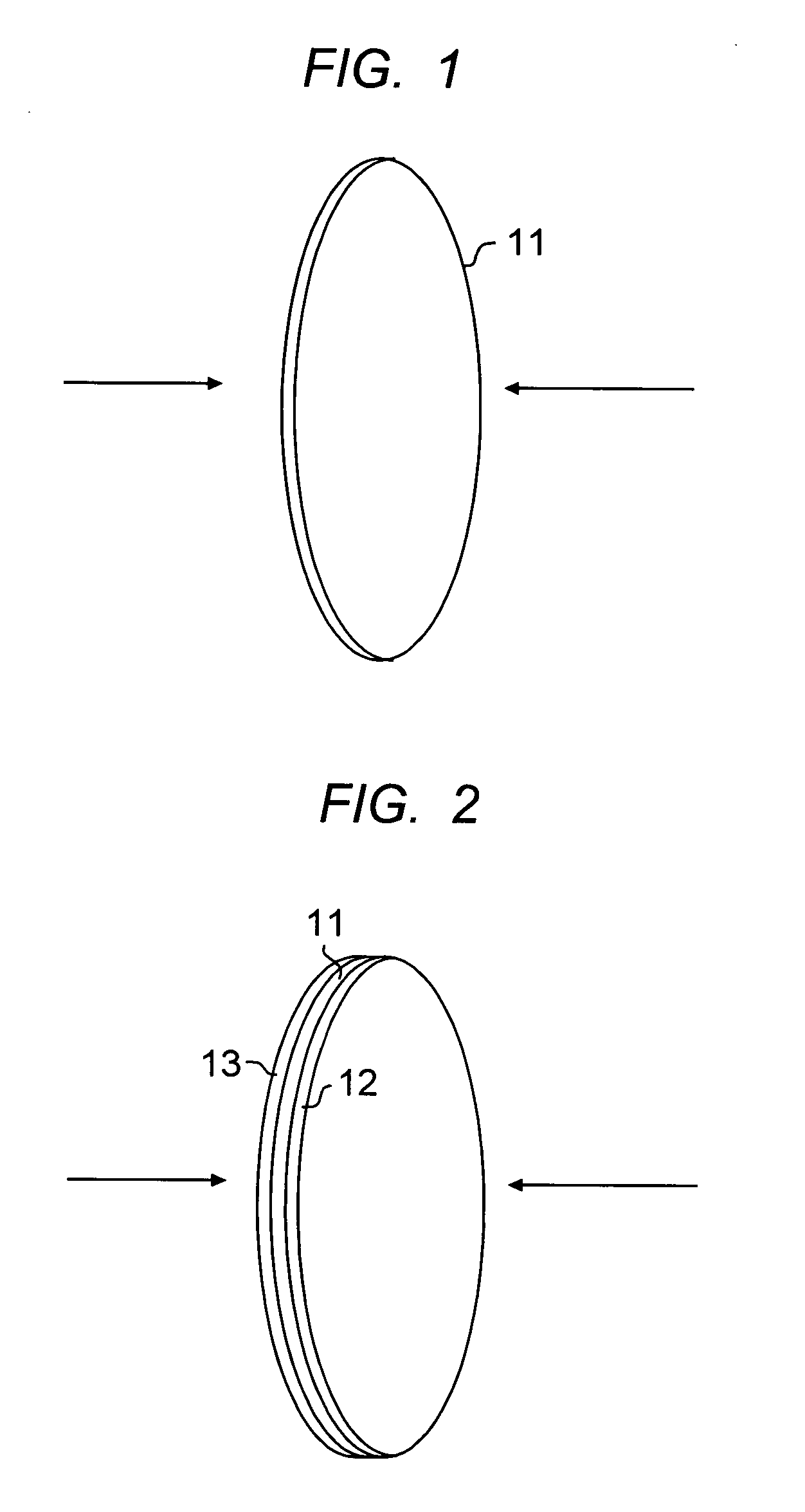
[0016]FIG. 1 is a view of the starting wafer 11. This is a single crystal silicon wafer cut from a boule, and is of a type of wafer used in enormous volume for IC device fabrication worldwide. Silicon wafers are produced in many sizes, but typically the larger the diameter of the wafer, the lower the potential device cost. Currently, silicon wafers are available in diameters up to twelve inches. With twelve inch wafers state of the art, that size will be used as the example in the following description, it being understood that smaller wafers, for example 6″ or 8″, are also useful.

[0017]In a wafer production facility, after sawing and polishing the wafers, each wafer is subjected to quality control, where the wafer is measured for conformity to rigid standards for physical size and electrical properties. Typically wafers with chips or scratches will be rejected. Wafers that have excessive or non-uniform conductivity are also rejected. In many cases the rejected wafers are scrapped, ...


PUM


Abstract

The specification describes an integrated passive device (IPD) that is formed on a polysilicon substrate. A method for making the IPD is disclosed wherein the polysilicon substrate is produced starting with a single crystal handle wafer, depositing a thick substrate layer of polysilicon on one or both sides of the starting wafer, forming the IPD on one of the polysilicon substrate layers, and removing the handle wafer. In a preferred embodiment the single crystal silicon handle wafer is a silicon wafer rejected from a single crystal silicon wafer production line.

Description

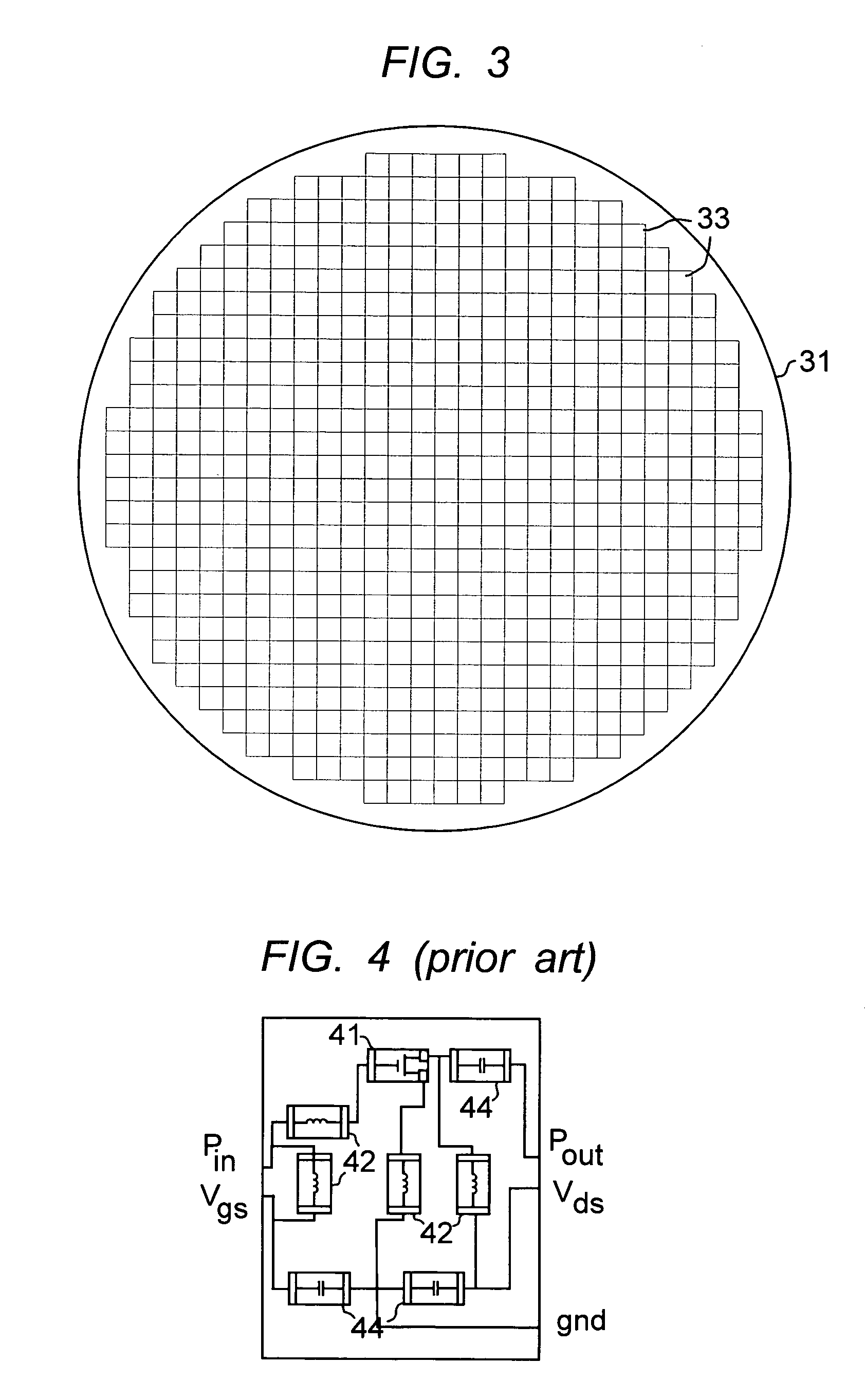
FIELD OF THE INVENTION[0001]This invention relates to integrated passive devices (IPDs) and more specifically to improved platforms for integrated passive device circuits.BACKGROUND OF THE INVENTION[0002](Portions of the technical material contained in this section may not be prior art.)[0003]State of the art radio frequency (RF) electrical circuits use large quantities of passive devices. Many of these circuits are used in hand held wireless products. Accordingly, miniaturization of passive devices and passive device circuits is an important goal in RF device technology.[0004]Integration and miniaturization of passive devices on the scale of active silicon devices has not occurred for at least two reasons. One, typical passive devices to date employ different material technologies. But, more fundamentally, the size of many passive devices is a function of the frequency of the device, and thus is inherently relatively large. However, still, there is unrelenting pressure to produce m...

Claims


Application Information

Patent Timeline
Patent Type & Authority Patents(United States)
IPC IPC(8): H01L21/20H01L27/04H01L21/00H01L21/02H01L21/822H01L21/8242H01L23/34H01L27/01
CPCH01L27/016H01L27/101H01L28/10H01L28/20H01L28/40H01L2924/0002H01L2924/00H01L27/04
Inventor DEGANI, YINONLAU, MAUREEN Y.TAI, KING LIEN
Owner SYCHIP
Why Eureka
Try Eureka