Approach to improve ellipsometer modeling accuracy for solving material optical constants N & K

a modeling accuracy and ellipsometer technology, applied in the field of optical measurements, can solve the problems of erroneous n and k values, unreliable mapping signatures, and destructive interference with radiation, and achieve the effect of more reliable and higher accuracy

Inactive Publication Date: 2007-08-21
TAIWAN SEMICON MFG CO LTD
View PDF13 Cites 12 Cited by
  • Summary
  • Abstract
  • Description
  • Claims
  • Application Information

AI Technical Summary

Benefits of technology

[0011]An objective of the present invention is to provide a more reliable method of determining optical constants n and k that has higher accuracy.
[0013]A still further objective is to provide a method for determining n and k that enables improved process control for patterning photoresists.

Problems solved by technology

The light that passes through the photoresist may reflect off underlying layers and pass through the photoresist a second time and can either constructively or destructively interfere with radiation that passes in the opposite direction.
The swing amplitude has a detrimental effect on the lithography process, especially if the magnitude is more than a few % of the average dose.
Unfortunately, the accuracy of the n and k values are strongly dependent on the application engineer's experience.
A wrong initial guess for the regression fitting in the modeling phase will turn out erroneous n and k values and unreliable mapping signatures.

Method used


Image

  • Approach to improve ellipsometer modeling accuracy for solving material optical constants N & K
  • Approach to improve ellipsometer modeling accuracy for solving material optical constants N & K
  • Approach to improve ellipsometer modeling accuracy for solving material optical constants N & K

Examples


first embodiment

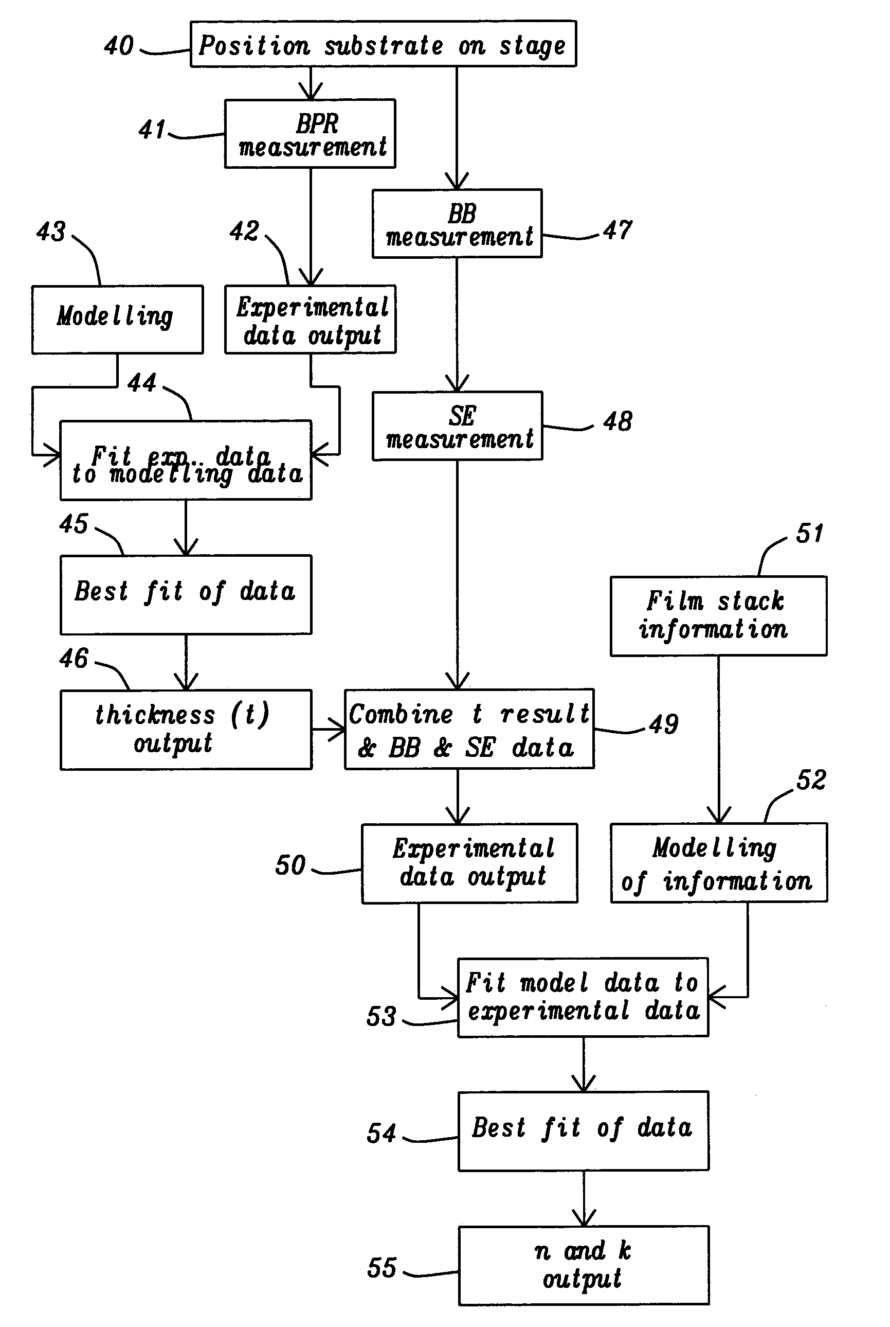
[0028]Table 1 indicates that an improvement in accuracy is achieved by determining thickness (t) in this manner compared to the prior art method of calculating n, k, and t simultaneously. In this example, layer 20 is a commercially available organic ARC. Using the traditional method as shown in FIG. 6, a thickness of 315.88 Angstroms is determined with a range of values of 15.97 Angstroms. By following a method described for the first embodiment, a thickness of 306.45 Angstroms and a range of 7.62 Angstroms is calculated. Since a smaller range corresponds to a higher degree of certainty in the measurement, a higher accuracy is realized with the present invention.

[0029]

TABLE 1Organic ARC thickness, n and k at 248 nmThicknessMethod(Angstroms)range(n)rangekrangeTraditional315.8815.971.83640.18350.62480.1481(n, k, t) all atonceThickness306.45 7.621.80780.02210.65580.0345first, thenn & k

[0030]Optionally, the integrated optical measurement system may include a Beam Profile Ellipsometry (B...

second embodiment

[0039]In a second embodiment, the invention is a method of characterizing n and k values of films in a multi-layer stack with greater accuracy than in prior art. Although several layers can be applied to construct a stack on a substrate, a description for measuring a two layer stack will be provided in this embodiment.

[0040]Referring to FIG. 5, a substrate 14 is provided as described in the first embodiment that is typically a silicon wafer. An organic or inorganic layer 20 hereafter referred to as underlayer 20 is deposited on the substrate 14 with an intended thickness in the range of about 300 to 10000 Angstroms. The underlayer 20 may be a commercially supplied material or an experimental formulation that is being optimized in a development mode. Moreover, the underlayer 20 may comprise an anti-reflective layer (ARC) or a photoresist that has been hard baked to a temperature of about 200° C. to 250° C. While a photoresist is normally applied in a spin-on process, an ARC may be fo...


PUM

PropertyMeasurementUnit
thicknessaaaaaaaaaa
wavelengthsaaaaaaaaaa
thicknessaaaaaaaaaa

Abstract

A method of determining optical constants n and k for a film on a substrate is described. Optical measurements are preferably performed with an integrated optical measurement system comprising a reflectometer, spectral ellipsometer, and broadband spectrometer such as an Opti-Probe series tool from Therma-Wave. A beam profile reflectometer is employed to first determine the thickness of said film from a best fit of modeling data to experimental data. The thickness data is combined with the ellipsometer and spectrometer measurements to produce an experimental data output which is fitted with modeled information to determine a best fit of the data. Constants n and k are derived from the best fit of data. The method provides a higher accuracy for n and k values than by standard procedures which calculate n, k, and t simultaneously. The method may also be applied to bilayer or multi-layer film stacks.

Description

FIELD OF THE INVENTION[0001]The invention relates to the field of optical measurements, and more particularly, to a method of determining film thickness and refractive index (n and k) from optical measurements taken with an integrated system including an ellipsometer, reflectometer, and spectrometer.BACKGROUND OF THE INVENTION[0002]Photolithography is a key component of semiconductor device manufacturing. A photosensitive composition that is often called a photoresist or resist is spin coated on a substrate and is patterned with a mask and an exposure system. The pattern is subsequently transferred into one or more underlying layers by a plasma etch method. Process control of the lithography step is crucial in order to maintain the critical dimension (CD) of features in the printed pattern within a specified range.[0003]Characterizing the optical properties and thickness of the photoresist and underlying layers is necessary to establish CD control. Typically, one or more wavelengths...

Claims


Application Information

Patent Timeline
Patent Type & Authority Patents(United States)
IPC IPC(8): G01J4/00G01N21/21G01N21/84
CPCG01N21/211G01N21/8422G01N2021/213
Inventor KE, CHIH-MINGCHEN, PEI-HUNGYU, SHINN-SHENG
Owner TAIWAN SEMICON MFG CO LTD
Why Eureka
Try Eureka