Processing of semiconductor components with dense processing fluids and ultrasonic energy

a technology of semiconductor components and processing fluids, applied in the direction of photomechanical treatment originals, cleaning using liquids, instruments, etc., can solve the problems of small contamination quantities, short circuits, open circuits, and other defects

Inactive Publication Date: 2007-09-11
AIR PROD & CHEM INC
View PDF74 Cites 21 Cited by
  • Summary
  • Abstract
  • Description
  • Claims
  • Application Information

AI Technical Summary

Benefits of technology

[0051](g) one or more processing agent storage vessels and pumping means to inject one or more processing agents (1) into the one or more pressurization vessels or (2) into the piping means for transferring the dense fluid from the one or more pressurization vessels to the sealable processing chamber or (3) into the sealable processing chamber.
[0052]T

Problems solved by technology

Small quantities of contamination are detrimental to the microchip fabrication process in the manufacturing of semiconductor electronic components.
Contamination in the form of particulates, films, or molecules causes short circuits, open circuits, silicon crystal stacking faults, and other defects.
These defects can cause the failure of finished microelectronic circuits, and such failures cause significant yield reductions, which greatly increases manufacturing costs.
Microelectronic circuit fabrication requires many processing steps.
Processing is performed under extremely clean conditions and the amount of contamination needed to cause fatal defects in microcircuits is extremely small.
For example, an individual particle as small as 0.01 micrometer in size can result in a killer defect in a modern microcircuit.
Also, tight control of purity and cleanliness of the processing materials is required.
As the device geometries shrink and gate oxide thickness decreases, sub-micrometer particle removal becomes increasingly difficult.
Wet processing methods may become problematic as microelectronic circuit dimensions decrease and as environmental restrictions increase.
Among the limitations of wet processing are the progressive contamination of re-circulated liquids, re-deposition from contaminated chemicals, special disposal requirements, environmental damage, special safety procedures during handling, reduced effectiveness in deeply patterned surfaces due to surface tension effects and image collapse (topography sensitivity), dependence of cleaning effectiveness on surface wet-ability t

Method used


Image

  • Processing of semiconductor components with dense processing fluids and ultrasonic energy
  • Processing of semiconductor components with dense processing fluids and ultrasonic energy
  • Processing of semiconductor components with dense processing fluids and ultrasonic energy

Examples


example 1

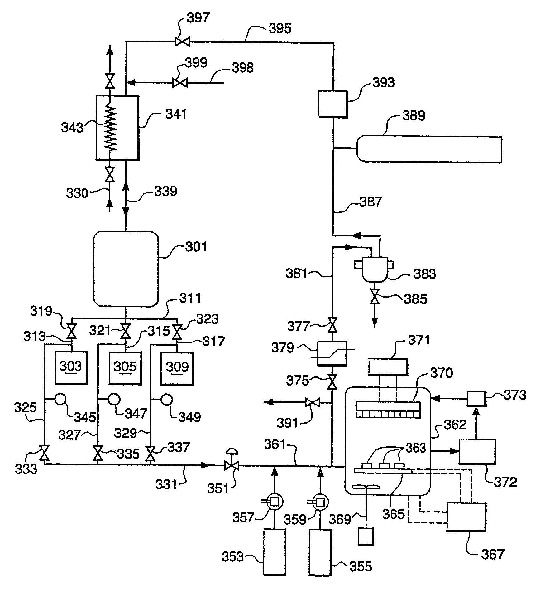
[0171]An embodiment of the invention according to FIG. 4 is used to treat a silicon wafer having a photoresist layer that has undergone multiple processing steps including exposure, development, etching and / or implantation with a dense processing fluid as described below.

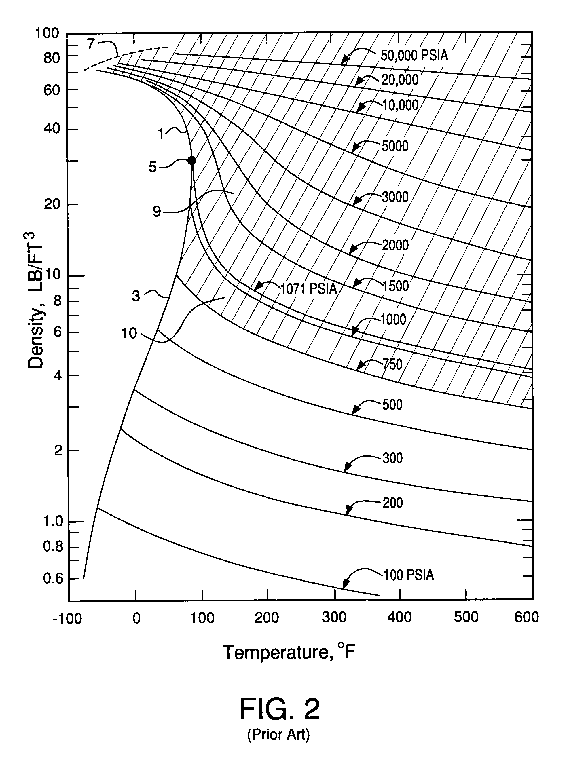
[0172]Step 1: Pressurization vessel 303 having a volume of 2.71 liters is filled completely with 4.56 lb of saturated liquid CO2 at 70° F. and 853.5 psia. The density of the initial CO2 charge is 47.6 lb / ft3. The vessel is sealed.

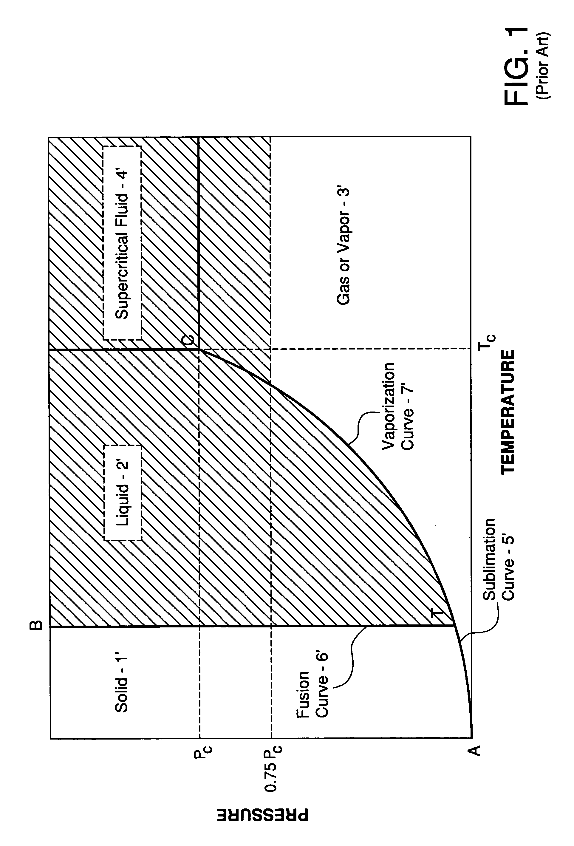
[0173]Step 2: The pressurization vessel is heated until the internal pressure reaches 5,000 psia. The density of the contained CO2 remains at 47.6 lb / ft3, and the temperature reaches 189° F. The contained CO2 is converted to a dense fluid in the supercritical region (see FIG. 2).

[0174]Step 3: A contaminated silicon wafer is loaded into process tool 362 having an interior volume of 1 liter. The process tool is evacuated and the vessel walls and wafer are held at 104° F.

[0175]Step 4: Valve 33...

example 2

[0181]The process of Example 1 is repeated except that ultrasonic transducer system 370 is operated during the cleaning period of step (5) at a sonic frequency which begins at 20 KHz and is increased at a constant rate during the cleaning period such that the sonic frequency is 200 KHz at the end of the cleaning period.

example 3

[0182]The process of Example 1 is repeated except that ultrasonic transducer 370 is operated during the cleaning period of step (5) at a sonic frequency which starts at 200 KHz and is decreased at a constant rate during the cleaning period such that the sonic frequency is 20 KHz at the end of the cleaning period.


PUM

PropertyMeasurementUnit
Fractionaaaaaaaaaa
Fractionaaaaaaaaaa
Fractionaaaaaaaaaa

Abstract

Method for processing an article with a dense processing fluid in a processing chamber while applying ultrasonic energy during processing. The dense fluid may be generated in a separate pressurization vessel and transferred to the processing chamber, or alternatively may be generated directly in the processing chamber. A processing agent may be added to the pressurization vessel, to the processing chamber, or to the dense fluid during transfer from the pressurization vessel to the processing chamber. The ultrasonic energy may be generated continuously at a constant frequency or at variable frequencies. Alternatively, the ultrasonic energy may be generated intermittently.

Description

CROSS-REFERENCE TO RELATED APPLICATIONS[0001]This application is a continuation-in-part of U.S. patent application Ser. No. 10 / 253,054, filed 24 Sep. 2002, now abandoned the disclosure of which is incorporated herein by reference in its entirety.BACKGROUND OF THE INVENTION[0002]Small quantities of contamination are detrimental to the microchip fabrication process in the manufacturing of semiconductor electronic components. Contaminants may be introduced into the component from many sources such as residues from manufacturing process steps such as lithography, etching, stripping, and chemical mechanical planarization (CMP); particulates either indigenous to and / or resulting from manufacturing processes; inorganic particulates or materials such as native or chemical oxides, metal-containing compounds; or other sources. Contamination in the form of particulates, films, or molecules causes short circuits, open circuits, silicon crystal stacking faults, and other defects. These defects c...

Claims


Application Information

Patent Timeline
IPC IPC(8): B08B7/04B01J3/00B01J19/10B08B3/08B08B3/12B08B7/00C11D7/24C11D7/26C11D7/32C11D7/50C11D11/00G03F1/00H01L21/00H01L21/304H01L21/306H01L21/311
CPCB08B3/12B08B7/0021C11D7/261C11D7/5013C11D7/5022C11D11/007H01L21/02052H01L21/31133C11D7/241C11D7/263C11D7/264C11D7/3209C11D7/3263C11D7/3281G03F1/82H01L21/67057H01L21/304
Inventor MCDERMOTT, WAYNE THOMASSUBAWALLA, HOSHANGJOHNSON, ANDREW DAVIDSCHWARZ, ALEXANDER
Owner AIR PROD & CHEM INC
Why Eureka
Try Eureka