Thick porous anodic alumina films and nanowire arrays grown on a solid substrate

a technology of porous anodic alumina and nanowire array, which is applied in the direction of crystal growth process, surface reaction electrolytic coating, metallic material coating process, etc., can solve the problems of limiting the active area of the film, limiting the use range of paa films, and affecting the stability of the film, etc., to achieve the effect of easy growth and more tractability

Inactive Publication Date: 2007-09-11
MASSACHUSETTS INST OF TECH
View PDF11 Cites 80 Cited by
  • Summary
  • Abstract
  • Description
  • Claims
  • Application Information

AI Technical Summary

Benefits of technology

[0010]The present new technology described herein allows for the fabrication of PAA films on a wide variety of substrates. The substrate comprises a wafer layer and may further include an adhesion layer deposited on the wafer layer. An alumina template is formed on the substrate. When a rigid substrate such as a conventional silicon wafer is used, the resulting anodic film is more tractable, easily grown on extensive areas in a uniform manner, and manipulated without danger of cracking. PAA films can also be grown this way on patterned and non-planar surfaces. Furthermore, under certain conditions the resulting PAA is missing the barrier layer (partially or completely) and the bottom of the pores can be readily accessed electrically The resultant film can be used as a template for forming an array of nanowires wherein the nanowires are prepared by filling the pores of the template by a different material The nanowires may be formed from various materials within the same template Arrays of nanowires may be stacked on top of each other into a multi-stage architecture.

Problems solved by technology

These disadvantages have precluded the use of PAA films in a wider range of applications.
Free-standing anodic films are extremely fragile and cannot sustain stress.
The mechanical polishing steps introduce imperfections and contamination, limit the active area of the film, and limit the throughput of the process.
Another disadvantage with the prior art process is that after the removal of the sustaining metal, the free-standing PAA film is very brittle and is hard to manipulate effectively.
Further, during the etch steps the surface topography of the film is degraded thereby affecting the optical properties of the film and its use as a mask.

Method used


Image

  • Thick porous anodic alumina films and nanowire arrays grown on a solid substrate
  • Thick porous anodic alumina films and nanowire arrays grown on a solid substrate
  • Thick porous anodic alumina films and nanowire arrays grown on a solid substrate

Examples


Embodiment Construction

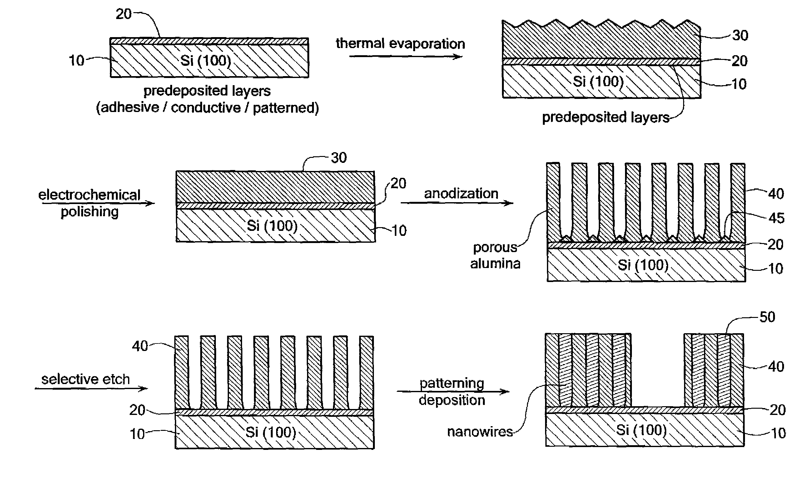
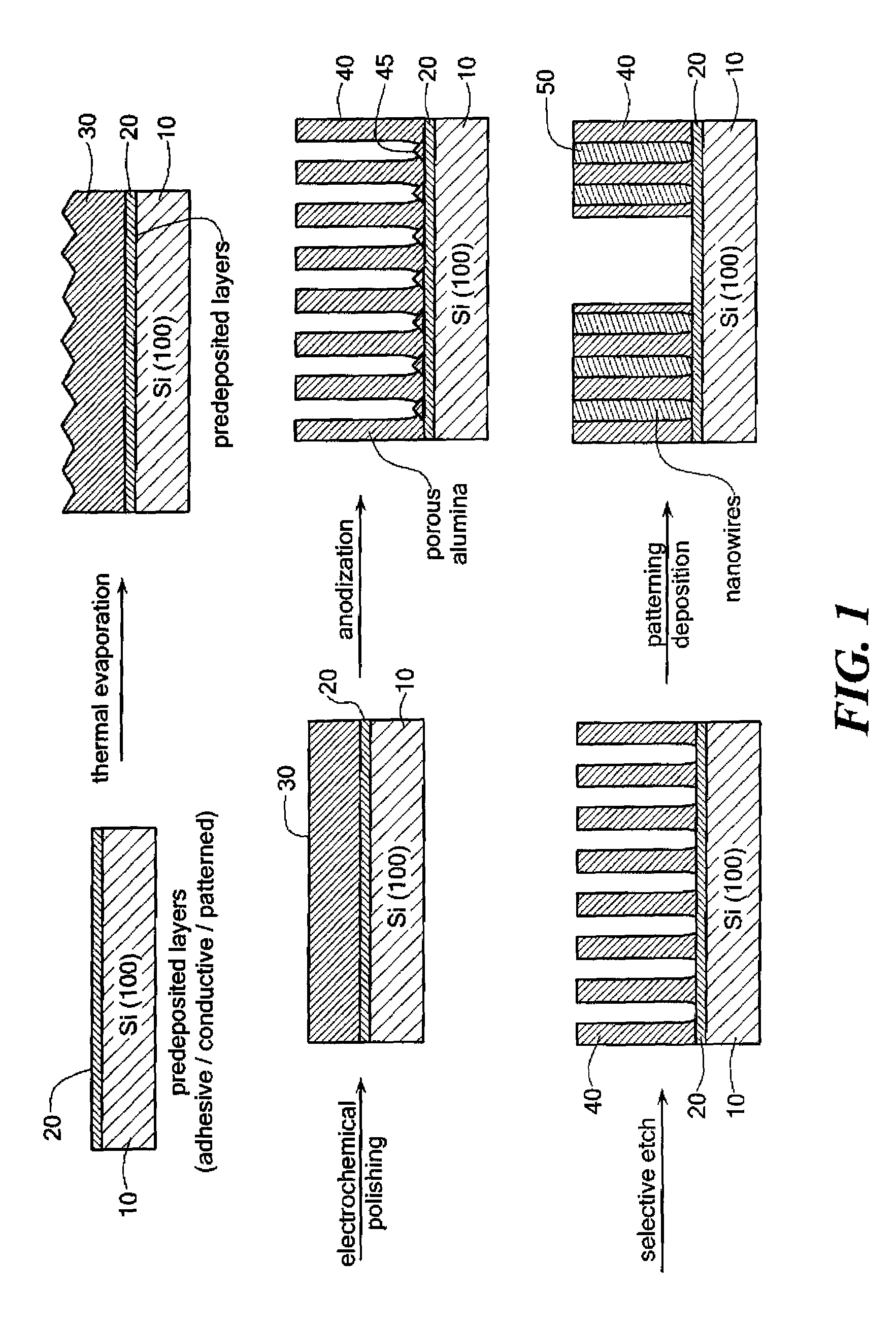
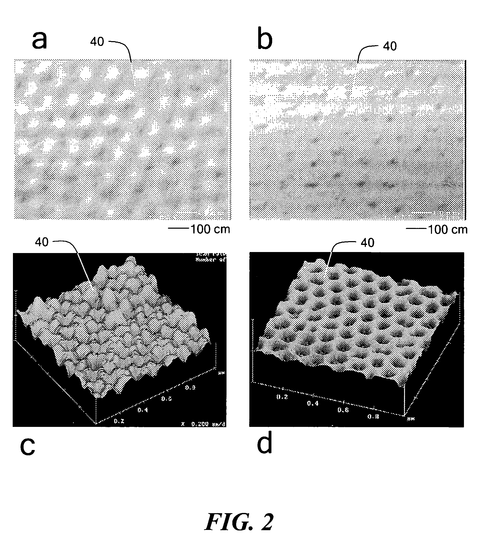
[0033]Porous anodic alumina (PAA) has received considerable attention as a template for the fabrication of nanostructures. The ordered triangular array of pores of high aspect ratio, whose dimensions can be accurately tuned by the process parameters, has made PAA a suitable host for the fabrication of nanowires of a wide range of materials. Applications of these arrays of nanowires include dense magnetic storage devices, field emission devices, thermoelectric devices, photovoltaic devices, nano-electrodes, sensing devices, photonic components and the study of low-dimensional quantum effects. Several researchers have used PAA as a mask for etching or deposition processes.

[0034]More recently, it was found that the optical properties of alumina together with the proper positioning of the voids in the film result in a 2-dimensional photonic crystal with a bandgap which can be controlled in the wavelength range of 520-600 nm (for certain polarizations and propagation directions of the li...


PUM

PropertyMeasurementUnit
thicknessaaaaaaaaaa
thicknessaaaaaaaaaa
surface roughnessaaaaaaaaaa

Abstract

The presently disclosed invention provides for the fabrication of porous anodic alumina (PAA) films on a wide variety of substrates. The substrate comprises a wafer layer and may further include an adhesion layer deposited on the wafer layer. An anodic alumina template is formed on the substrate. When a rigid substrate such as Si is used, the resulting anodic alumina film is more tractable, easily grown on extensive areas in a uniform manner, and manipulated without danger of cracking. The substrate can be manipulated to obtain free-standing alumina templates of high optical quality and substantially flat surfaces PAA films can also be grown this way on patterned and non-planar surfaces. Furthermore, under certain conditions the resulting PAA is missing the barrier layer (partially or completely) and the bottom of the pores can be readily accessed electrically. The resultant film can be used as a template for forming an array of nanowires wherein the nanowires are deposited electrochemically into the pores of the template. By patterning the electrically conducting adhesion layer, pores in different areas of the template can be addressed independently, and can be filled electrochemically by different materials. Single-stage and multi-stage nanowire-based thermoelectric devices, consisting of both n-type and p-type nanowires, can be assembled on a silicon substrate by this method.

Description

RELATED APPLICATIONS[0001]This application claims priority under 35 U.S.C. § 119(e) to provisional patent application Ser. No. 60 / 333,403 filed Nov. 26, 2001; the disclosure of which is incorporated by reference herein.GOVERNMENT RIGHTS[0002]This invention was made with Government support under Contract No. 0205-G-BB853, awarded by MURI / ONR / UCLA, Contract No. N00167-98-K-0024 awarded by the Department of the Navy, Contract No. N00014-96-1-0802 awarded by the Department of the Navy and DARPA, Subcontract No 0205-G-7A114 awarded by MURI, and Grant No DMR-98-04734 awarded by NSF. The Government has certain rights in this invention.FIELD OF THE INVENTION[0003]The present invention relates generally to porous anodic alumina films and more specifically to a method and apparatus incorporating porous anodic alumina films as a template for the fabrication of nanostructured devices.BACKGROUND OF THE INVENTION[0004]Porous anodic alumina (PAA) films are films generated by electrochemical oxidat...

Claims


Application Information

Patent Timeline
Patent Type & Authority Patents(United States)
IPC IPC(8): B32B3/10B32B15/00B32B9/00C23C28/00G03C5/00C30B7/00H01L35/32H01L35/34
CPCB82Y30/00C23C14/16C23C14/5873C30B7/00H01L35/32H01L35/34C23C14/024C30B7/005C30B29/605Y10T428/1259Y10T428/12486Y10T428/24273Y10T156/10Y10T428/24917Y10T428/24322H10N10/01H10N10/17
Inventor RABIN, ODEDHERZ, PAUL R.DRESSELHAUS, MILDRED S.AKINWANDE, AKINTUNDE I.LIN, YU-MING
Owner MASSACHUSETTS INST OF TECH
Why Eureka
Try Eureka