Digital BIST test scheme for ADC/DAC circuits

a digital bist and circuit technology, applied in the field of test circuits, can solve the problems of inability, high cost, and limited capacity of analog testers, and achieve the effect of accurately testing the analog portion of the chip

Inactive Publication Date: 2007-09-18
TOSHIBA AMERICA ELECTRONICS COMPONENTS
View PDF4 Cites 26 Cited by
  • Summary
  • Abstract
  • Description
  • Claims
  • Application Information

AI Technical Summary

Benefits of technology

[0007]In accordance with an aspect of the present invention, there is described herein a system and method that provides the ability to accurately test an analog portion of a chip using a digital tester. An aspect of the present invention is that a chip can be tested once to verify the integrity of the digital and analog components.
[0008]In accordance with an aspect of the present invention, there is described herein a generalized method of testing voltage output DACs (Digital to Analog Converters) and ADCs (Analog to Digital Converters), such as Sigma Delta (Successive Approximation), Pipeline or Flash ADCs. The DACs and ADCs are tested in pairs using a Digital Tester and on chip test circuitry. The DACs and ADCs may be tested at the highest clock frequency allowed in the specification, shortening test time. The test circuits required for this test scheme comprise cell logic, two analog multiplexer cells and an internal Analog Test Bus. This scheme is extendable to the testing of many DACs and ADCs on the same IC. The number of DACs and ADCs need not be equal. Furthermore, the DACs may have more (or less) bits (addresses) than the ADCs. An ADC may be tested with more than one DAC or vice versa to determine which cell is at fault if a test fails.

Problems solved by technology

If the device response and the expected response are not in agreement, the device is usually considered defective.
In a typical semiconductor manufacturing environment, there are usually a plethora of digital testers available, but few analog testers.
This is because analog testers are usually limited in number, limited in capability and can be more expensive than digital testers.
Furthermore, the analog test function can be slow.

Method used


Image

  • Digital BIST test scheme for ADC/DAC circuits
  • Digital BIST test scheme for ADC/DAC circuits
  • Digital BIST test scheme for ADC/DAC circuits

Examples


Embodiment Construction

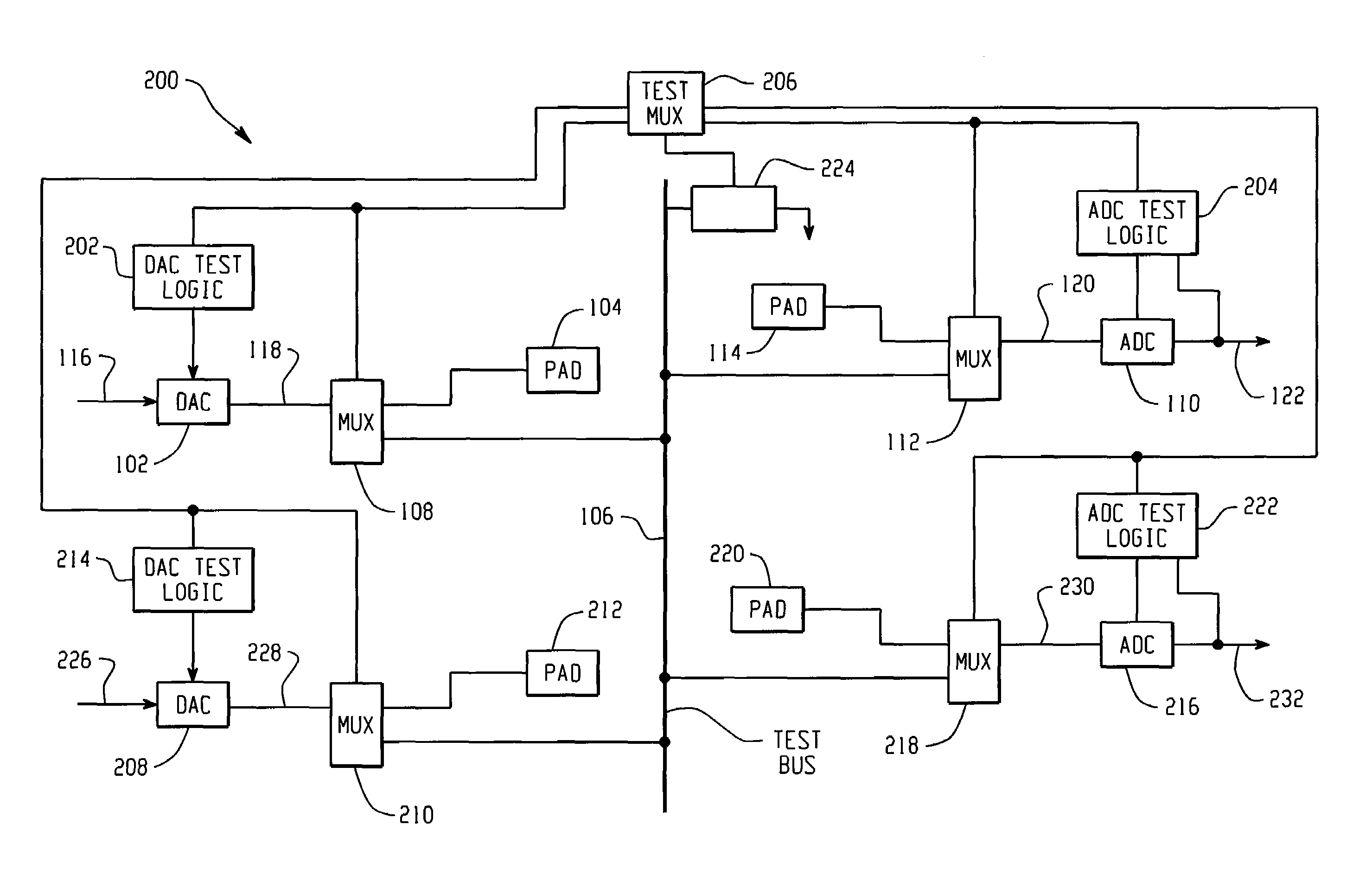
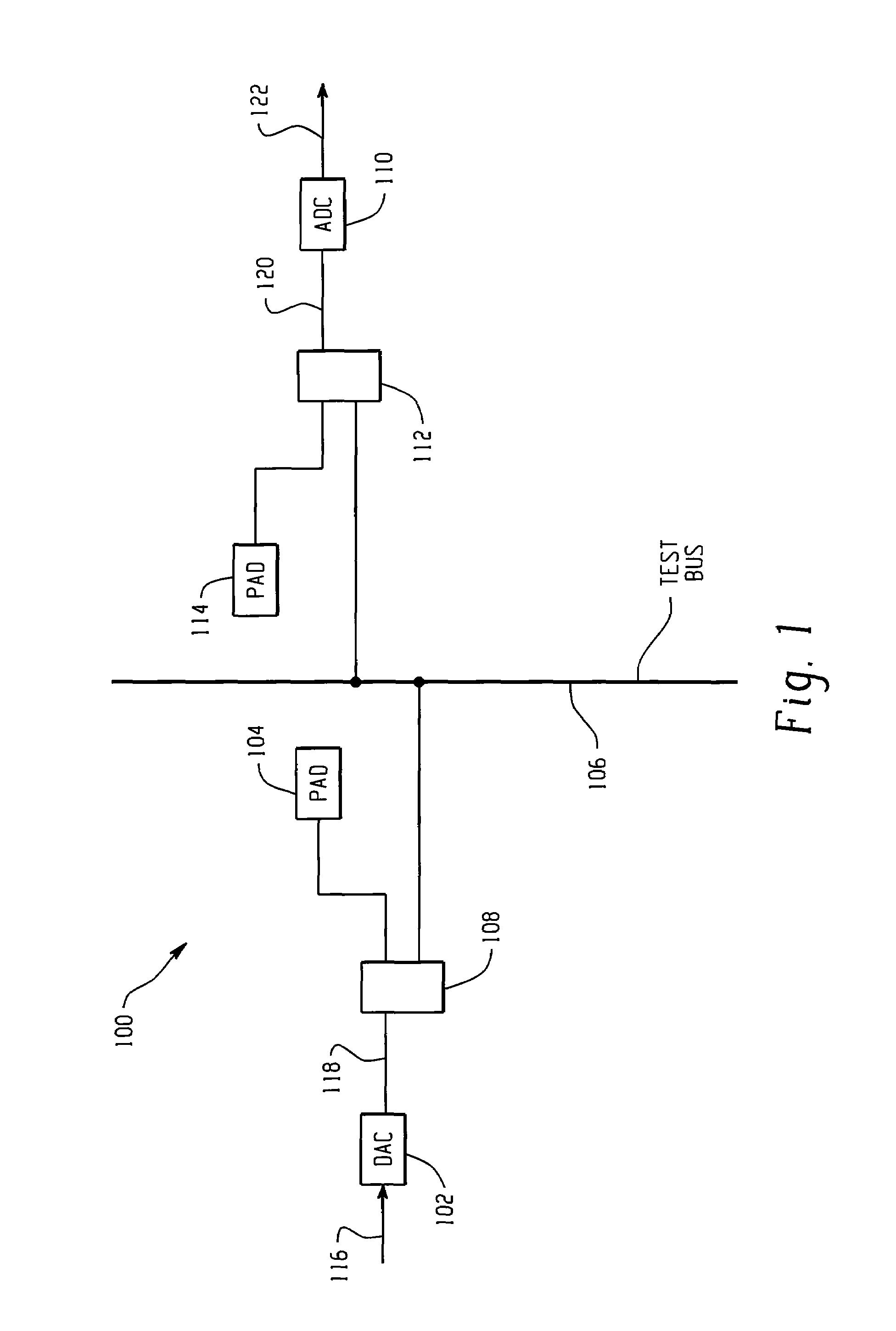
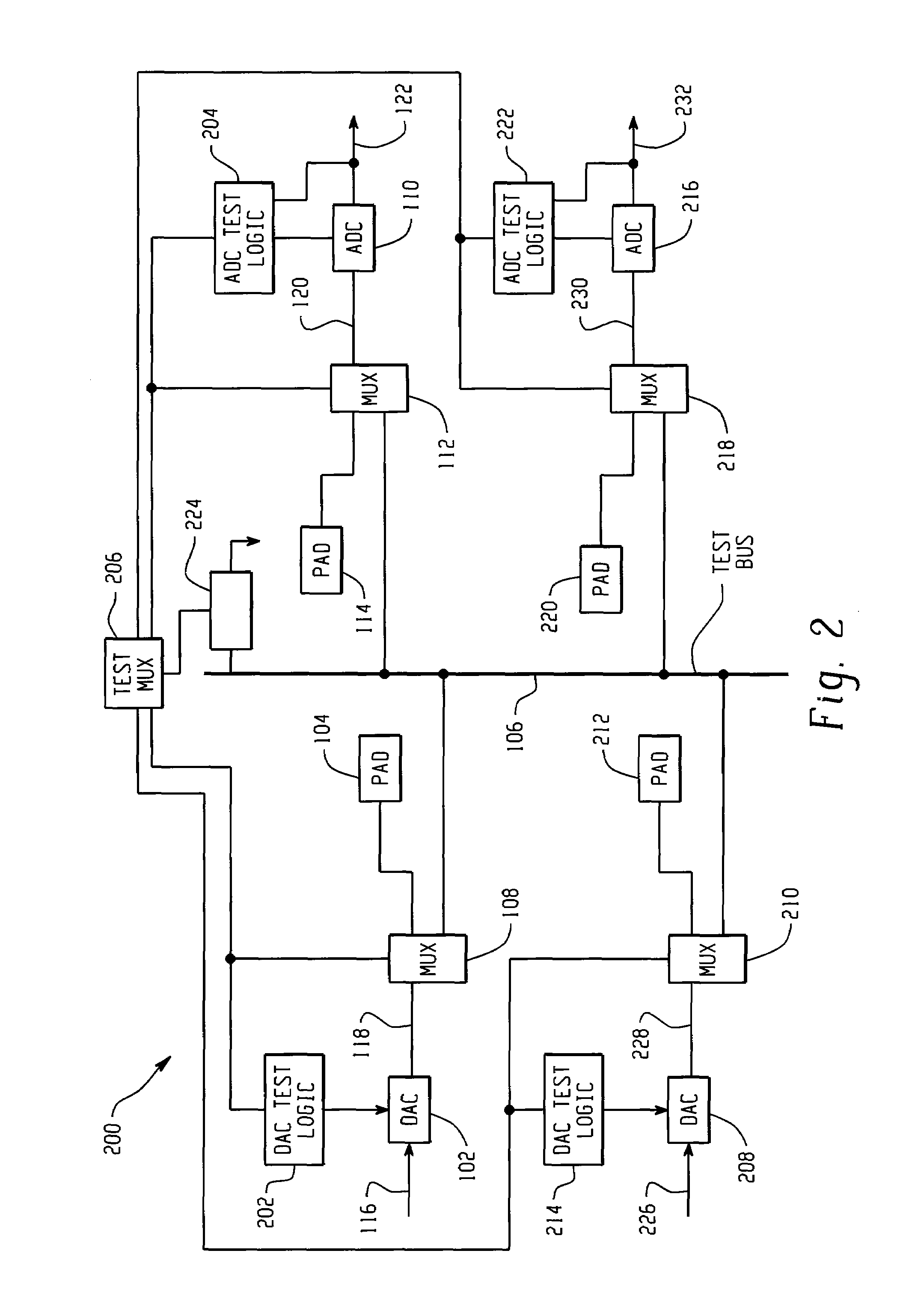
[0035]Throughout this description, the preferred embodiment and examples shown should be considered as exemplars, rather than limitations, of the present invention. Like reference numbers refer to like components. Described herein is a generalized method of testing voltage output DACs and Sigma Delta (Successive Approximation), Pipeline or Flash ADCs. The DACs and ADCs are tested in pairs using only a Digital Tester and on chip test circuitry. The DACs and ADCs may be tested at the highest clock frequency allowed in the specification, shortening test time. The test circuits required for this test scheme consist of standard cell logic with the exception of two additional ‘analog’ IO mux cells and an internal Tristate Analog Test Bus. This scheme is extendable to the testing of many DACs and ADCs on the same IC. The number of DACs and ADCs need not be equal. The DACs may have more bits (addresses) than the ADCs. An ADC may be tested with more than one DAC or vice versa to determine wh...


PUM


Abstract

A generalized method for testing DACs (Digital to Analog Converters) and ADCs (Analog to Digital Converters), such as Sigma Delta (Successive Approximation), Pipeline or Flash ADCs. The DACs and ADCs are tested in pairs using a Digital Tester and on chip test circuitry. The DACs and ADCs may be tested at the highest clock frequency allowed in the specification, shortening test time. The test circuits required for this test scheme comprise cell logic two multiplexer cells and an internal Analog Test Bus. This scheme is extendable to the testing of many DACs and ADCs on the same IC. The number of DACs and ADCs need not be equal. Furthermore, the DACs may have more (or less) bits (addresses) than the ADCs. An ADC may be tested with more than one DAC or vice versa to determine which cell is at fault if a test fails.

Description

BACKGROUND OF THE INVENTION[0001]The present invention relates generally to test circuits and more specifically to a system and method for performing a digital built in self test (BIST) of Analog to Digital (ADC) and Digital to Analog (DAC) circuits.[0002]The function of test of a semiconductor device is twofold. First, is design debug, to understand the failing section of the device, identify areas for changes and verify correct modes of operation. The second major area is to simply separate good devices from bad devices in a production test environment.[0003]The basis for all testing of complex integrated circuits is a comparison of known good patterns to the response of a DUT (device under test). The simulation of the devices is done with input stimuli and those same input stimuli (vectors) are presented on the DUT. Comparisons are made cycle by cycle with an option to ignore certain pins, times or patterns. If the device response and the expected response are not in agreement, t...

Claims


Application Information

Patent Timeline
Patent Type & Authority Patents(United States)
IPC IPC(8): H03M1/10
CPCH03M1/1071H03M1/12H03M1/66
Inventor PETERSON, LUVERNELEVI, JONATHAN A.ABELOVSKI, PAULMAR, ROGER
Owner TOSHIBA AMERICA ELECTRONICS COMPONENTS
Why Eureka
Try Eureka