Analog to digital converter

a converter and analog technology, applied in analogue/digital conversion, transmission systems, instruments, etc., can solve the problems of high conversion speed, limited resolution, increased cost, etc., and achieve the effect of improving recovery from conversion errors

Active Publication Date: 2007-09-25
ANALOG DEVICES INC
View PDF22 Cites 15 Cited by
  • Summary
  • Abstract
  • Description
  • Claims
  • Application Information

AI Technical Summary

Benefits of technology

[0017]It is thus possible to provide an improved analog to digital converter in which the analog to digital conversion is done in first and second stages. This has a first advantage that a complete conversion need not be performed before starting the next analog to digital conversion. Thus, in a converter having first and second converter cores, the second converter core could be finishing an analog to digital conversion whilst the first converter core is switched to a tracking mode such that it acquires the next analog sample to be converted. Alternatively the first ADC, in addition to tracking and sampling the new input, may also commence converting the new input whilst the second converter is still converting the previous input. A second advantage of performing the conversion in two stages is that although miss-match between collaborative ADCs may limit the number of bits that can be converted in each of the first and second converter cores to about 10 bits of resolution, the overall converter may be now have a resolution close to 20 bits, the resolution of both converters combined. The first and second conversion cores could be implemented using any one of a number of implementing technologies, although FLASH converters and successive approximation converters are preferred. As a further enhancement to throughput, at least one, and preferably both the first and second converter cores comprise at least three successive approximation converter engines arranged in parallel and operating in a co-operative manner such that each successive conversion cycle within a single converter core can determine two bits simultaneously.
[0034]As noted before, the conversion engines are generally made smaller so that a plurality of them can be provided without a corresponding increase in power consumption occurring. However making the capacitors within the sampling digital to analog converter stage of the ADC smaller gives rise to an increase in thermal noise. However, by connecting the individual outputs of the capacitor stages within the conversion engines in parallel, when generating the residue, the net thermal noise is reduced because the effective capacitance that determines the thermal noise is then the total capacitance of the individual ADCs.

Problems solved by technology

These objectives are generally opposed, and become more difficult to achieve when a user also seeks for such devices to be relatively inexpensive.
Flash converters are known to provide high conversion speed, albeit at increased cost and with limited resolution.
The formation of this number of comparators can result in a relatively power hungry device having a relatively large input capacitance.
These all result from the fact that in the real world components and systems are noisy.
This noise may come via the power supply lines, or it may be self generated thermal noise.
The first option, that is tripling the die area and the power consumption is generally not favoured as it makes the device more expensive to manufacture and less likely to be adopted by users as it eats into their power budget, which is particularly important in the context of mobile devices which are battery powered.
However simply making the individual converters smaller carries a noise penalty.
It could therefore be seen that smaller capacitors have greater thermal noise appearing at their terminals.
In the arrangement of U.S. Pat. No. 6,239,734 thermal noise occurring at any one of the successive approximation converters can result in that converter giving a false result and will skew the entire conversion process.
This probably does not represent an issue with the context of the 6-bit of the converter, but with modern converters requiring 12-bit or greater accuracy, the presence of self generated noise is now a significant factor in analog to digital converter design.

Method used


Image

  • Analog to digital converter
  • Analog to digital converter
  • Analog to digital converter

Examples


Embodiment Construction

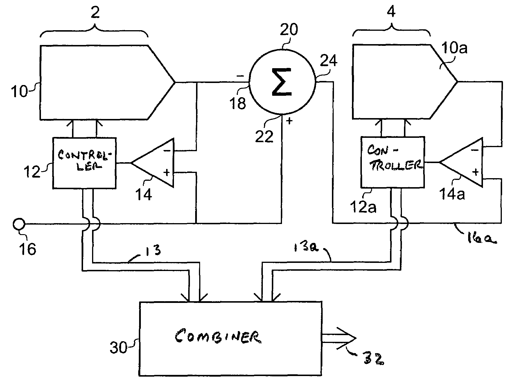
[0053]FIG. 1 schematically illustrates an analog to digital converter constituting an embodiment of the invention. In essence two converter cores, generally labelled 2 and 4 (each comprising an analog-to-digital converter with both a digital output and an output supplying an analog representation of that digital output) are provided in series. The conversion task is split between the converters such that the first converter core 2 converts a first and most significant portion of the analog signal, for example the equivalent of the upper six to nine bits of a 16-bit word, and the second converter core 4 determines the remaining portion equivalent to, for example, the least significant bits of the analog to digital conversion.

[0054]In a preferred embodiment of the present invention both converter cores 2 and 4 are implemented as successive approximation converters. The converter cores 2 and 4 will be described in detail later. This allows each converter core to be relatively accurate ...


PUM


Abstract

A analog to digital converter, comprising: an input for receiving an input signal to be digitized; a first converter core for performing a first part of an analog to digital conversion, and for outputting a first digital result; a first residue calculator for calculating a first residue as a difference between the input signal and the first digital result; a second converter core for performing a second part of the analog to digital conversion by converting the first residue; wherein at least one of the first and second converter cores comprises at least three analog to digital conversion engines and a controller for controlling the operation of the engines such that the engines collaborate to perform a successive approximation search, and wherein a plurality of bits can be determined during a single trial step of the successive approximation search.

Description

FIELD OF INVENTION[0001]The present invention relates to an analog to digital converter using a plurality of conversion cores, at least one of which comprises plurality of conversion engines acting in a co-operative state to allow multiple bits to be examined at each trial.BACKGROUND OF THE INVENTION[0002]Users of analog to digital converters generally wish to see high conversion accuracy and high conversion rates. These objectives are generally opposed, and become more difficult to achieve when a user also seeks for such devices to be relatively inexpensive.[0003]Flash converters are known to provide high conversion speed, albeit at increased cost and with limited resolution. In essence a flash converter consists of a plurality of comparators, each comparator connected to a respective tap on a resistor chain such that each comparator is responsible for testing for one, and only one, of the possible digital outputs. Therefore an 8 bit flash converter requires 255 individual comparat...

Claims


Application Information

Patent Timeline
Patent Type & Authority Patents(United States)
IPC IPC(8): H03M1/12
CPCH03M1/145H03M1/144H03M1/468
Inventor HURRELL, CHRISTOPHER PETERLYDEN, COLIN GERARD
Owner ANALOG DEVICES INC
Why Eureka
Try Eureka