Method of mounting electronic component, structure for mounting electronic component, electronic component module, and electronic apparatus

Active Publication Date: 2007-10-09
BOE TECH GRP CO LTD
View PDF17 Cites 6 Cited by
  • Summary
  • Abstract
  • Description
  • Claims
  • Application Information

AI Technical Summary

Benefits of technology

[0033]On the other hand, an electronic component module according to the present invention includes any one of the above-mentioned structures of mounting the electronic component. By this configuration, the electronic component module having the above-mentioned

Problems solved by technology

In addition, since the clearances of the electronic pads have narrowed and the electrode pad itself is so small, the number of the conductive particles captured by each electrode p

Method used


Image

  • Method of mounting electronic component, structure for mounting electronic component, electronic component module, and electronic apparatus
  • Method of mounting electronic component, structure for mounting electronic component, electronic component module, and electronic apparatus
  • Method of mounting electronic component, structure for mounting electronic component, electronic component module, and electronic apparatus

Examples


first exemplary embodiment

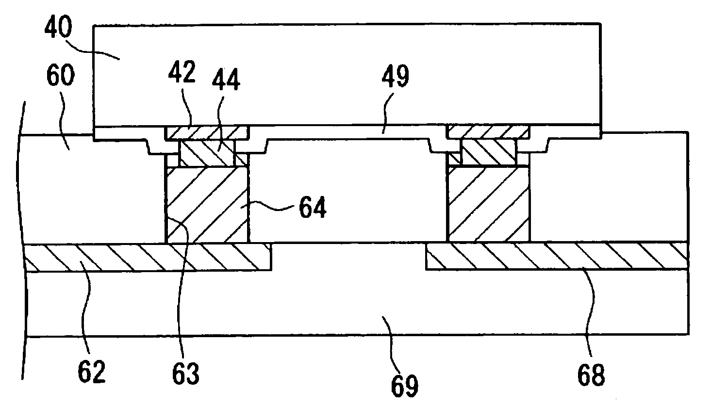
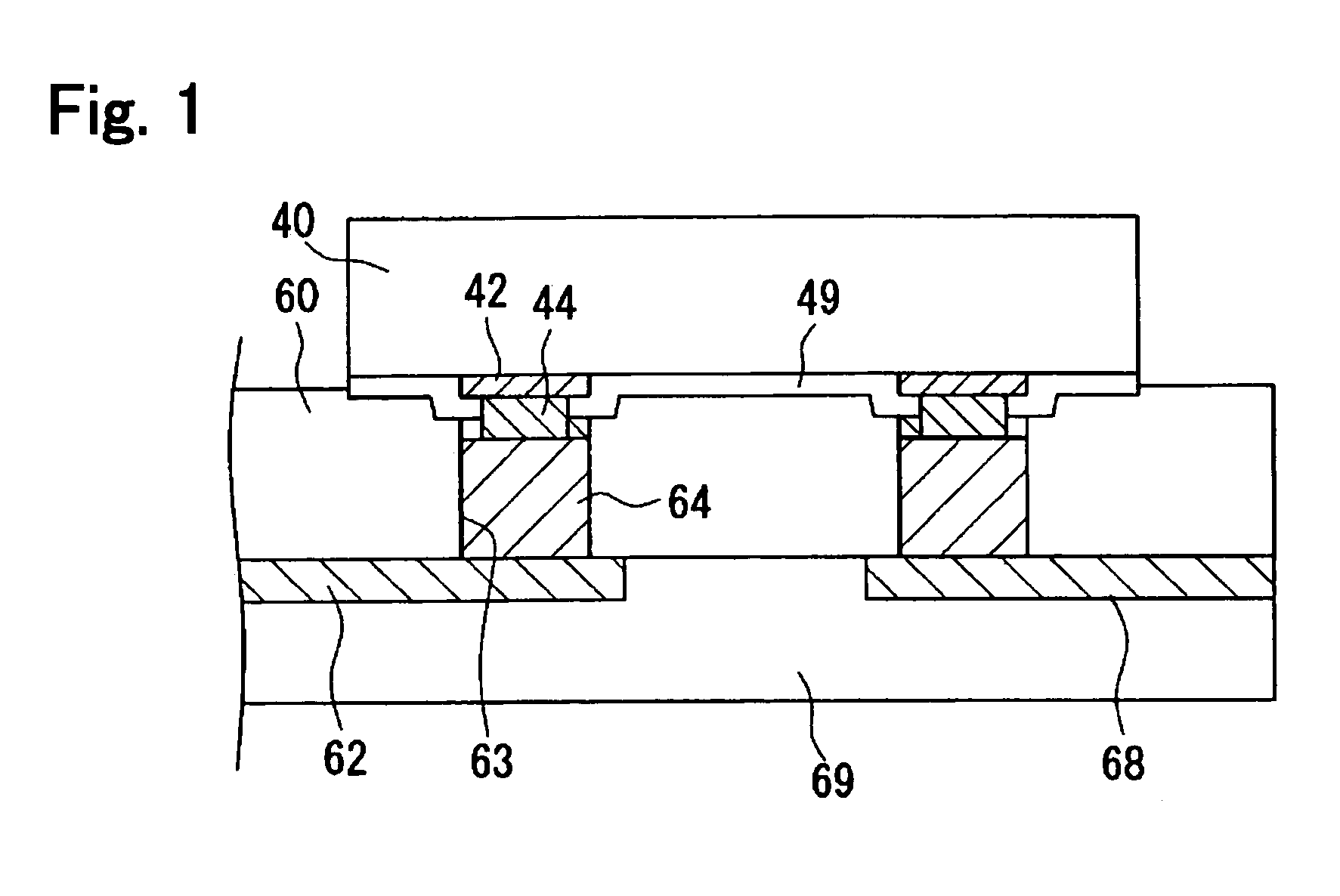
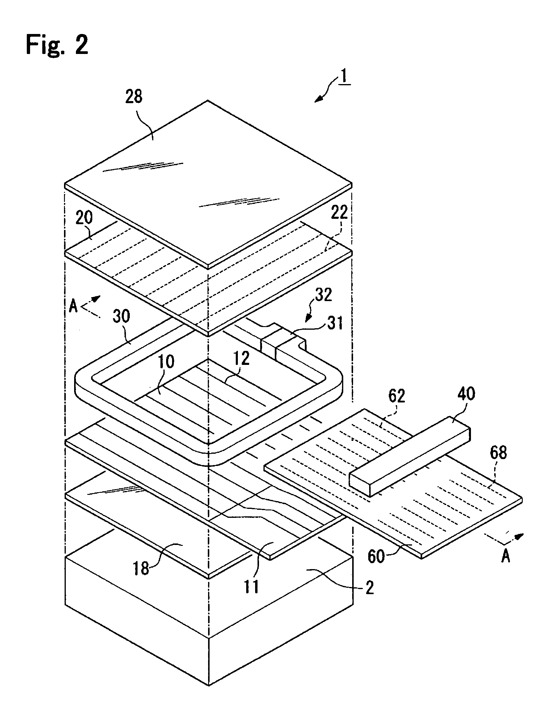
[0043]First, the structure and method of mounting an electronic component according to the first exemplary embodiment is described. A liquid crystal display device, which is the electronic component module mounted with an IC as the electronic component, is explained with reference to FIGS. 2 and 3. In addition, FIG. 2 is an exploded perspective view of the liquid crystal display device, and FIG. 3 is a cross-sectional side view taken along plane A-A of FIG. 2. In addition, although in the present exemplary embodiment, a passive matrix type liquid crystal display device is explained as an example, the present invention can be applied to an active matrix type liquid crystal display device. Further, FIGS. 2 and 3 schematically show the liquid crystal display device, but an actual liquid crystal display device is formed of a plurality of various electrodes and terminals.

Exemplary Liquid Crystal Display Device

[0044]As shown in FIG. 2, in the liquid crystal display device 1 according to t...

second exemplary embodiment

[0065]Next, the structure and method of mounting the electronic component according to the second exemplary embodiment is described using FIG. 5. The second exemplary embodiment is different from the first exemplary embodiment in that the conductive thermosetting resin 65 fills in the through-hole 63 of the FPC 60. In addition, the detailed description about the same portion as that of the first exemplary embodiment is omitted.

[0066]In the structure to mount the electronic component according to the second exemplary embodiment, the conductive thermosetting resin 65 fills in the through-hole 63 of the FPC 60. As the thermosetting resin 65 has conductivity, the thermosetting resin 65 containing metal powder is used. It is preferable that epoxy resin be used as the thermosetting resin. In addition, it is preferable that fine particle, such as silver (Ag), gold (Au) or nickel (Ni), be used as metal powder. The thermosetting resin 65 has conductivity by dispersing the metal powder to the...


PUM

PropertyMeasurementUnit
Temperatureaaaaaaaaaa
Melting pointaaaaaaaaaa

Abstract

The invention provides a method of mounting an electronic component where an electronic component can be reliably electrically-connected to a substrate. A substrate defines a through-hole that extends through the substrate, from connection electrodes formed on the lower surface of the substrate, to the upper surface of the substrate. A low melting point metal is connected to the connection electrodes and fills the through-hole. A bump and the low melting point metal are alloyed and bonded by heating the low melting point metal while pressing the bump formed on an electrode pad of an electronic component, with respect to a front end of the low melting point metal. The active surface of the electronic component is sealed by the upper surface of the substrate.

Description

BACKGROUND OF THE INVENTION[0001]1. Field of Invention[0002]The present invention relates to a method of mounting an electronic component, a structure to mount an electronic component, an electronic component module, and an electronic apparatus.[0003]2. Description of Related Art[0004]An electronic component, such as an integrated circuit IC, can be used after being mounted on a circuit board. The related art includes various methods of mounting the electronic component on the circuit board. FIGS. 7(a) and 7(b) show a structure to mount an electronic component according to the related art. In FIG. 7(a), the electronic component 170, such as an IC, is mounted on the substrate 120 with an anisotropic conductive film (ACF) 190 sandwiched in between them. The anisotropic conductive film 190 disperses conductive particles 195 in a thermosetting resin 192. The conductive particles 195 are inserted between electrode pads 172 formed on an active surface of the electronic component 170 and e...

Claims


Application Information

Patent Timeline
IPC IPC(8): B23K31/00B23K31/02H05K3/32H01L21/60H01L23/13H01L23/498H05K1/02H05K1/11H05K1/18H05K3/34H05K3/40
CPCH01L23/13H01L23/49827H01L24/81H01L24/83H05K1/112H01L24/29H01L2224/13147H01L2224/16225H01L2224/16237H01L2224/73204H01L2224/81801H01L2224/8319H01L2224/838H01L2924/01004H01L2924/01005H01L2924/01013H01L2924/01029H01L2924/0103H01L2924/01033H01L2924/01047H01L2924/01049H01L2924/0105H01L2924/01074H01L2924/01078H01L2924/01079H01L2924/0781H01L2924/14H01L2924/3025H05K3/4038H05K3/4069H05K2201/0305H05K2201/0394H05K2201/09472H05K2201/10674H01L2924/0132H01L2224/2919H01L2924/01006H01L2924/014H01L2924/0665H01L2224/29101H01L2924/0133H01L2224/2929H01L2224/29109H01L2224/29111H01L2224/13111H01L2224/29339H01L2224/29344H01L2224/29355H01L2224/16235H01L2924/00H01L2924/00014H01L2924/12042H01L2224/05573H01L2224/05599H05K3/34
Inventor SAITO, ATSUSHI
Owner BOE TECH GRP CO LTD
Why Eureka
Try Eureka