Reactor for extended duration growth of gallium containing single crystals
What is Al technical title?
Al technical title is built by PatSnap Al team. It summarizes the technical point description of the patent document.
a gallium-containing single crystal, extended-duration technology, applied in the direction of crystal growth process, polycrystalline material growth, chemically reactive gas, etc., can solve the problem of relatively low growth rate at this temperature, and achieve the effect of extended growth cycles, controllable and limited amount of ga undergoing a reaction
Inactive Publication Date: 2007-10-09
OSTENDO TECH INC
View PDF64 Cites 35 Cited by
Summary
Abstract
Description
Claims
Application Information
AI Technical Summary
This helps you quickly interpret patents by identifying the three key elements:
Problems solved by technology
Method used
Benefits of technology
[0016]According to one aspect of the invention, an extended Ga source is located within a reactor such that a portion of the Ga source is maintained at a relatively high temperature while most of the Ga source is maintained at a temperature close to, and just above, the melting temperature of Ga. In at least one embodiment of the invention, in order to obtain the desired temperature spread in the Ga source, a portion of the source tube extends outside of the reactor. Assuming the use of a modified HVPE process for the growth of the single crystal boule, preferably the high temperature is in the range of 450° C. to 850° C., and more preferably at a temperature of approximately 650° C., while the low temperature is less than 100° C. and preferably in the range of 30° C. to 40° C. As a result of this source configuration, the amount of Ga undergoing a reaction is controllable and limited, thus allowing extended growth cycles to be realized without experiencing degradation in the as-grown material.
Problems solved by technology
Although the high temperature of this zone allows high quality crystal growth, the growth rate at this temperature is relatively low.
Method used
Image
Click on the blue label to locate the original text in one second.
Reading with bidirectional positioning of images and text.
Examples
specific embodiments
[0052]Embodiment 1
[0053]According to this embodiment of the invention, the modified HVPE process described above was used to grow thick GaN layers on SiC substrates. Suitable GaN substrates were then fabricated and used in conjunction with the modified HVPE process of the invention to grow a GaN single crystal boule. The second GaN boule was cut into wafers suitable for device applications.
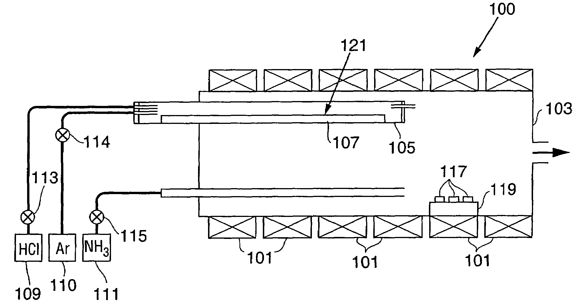
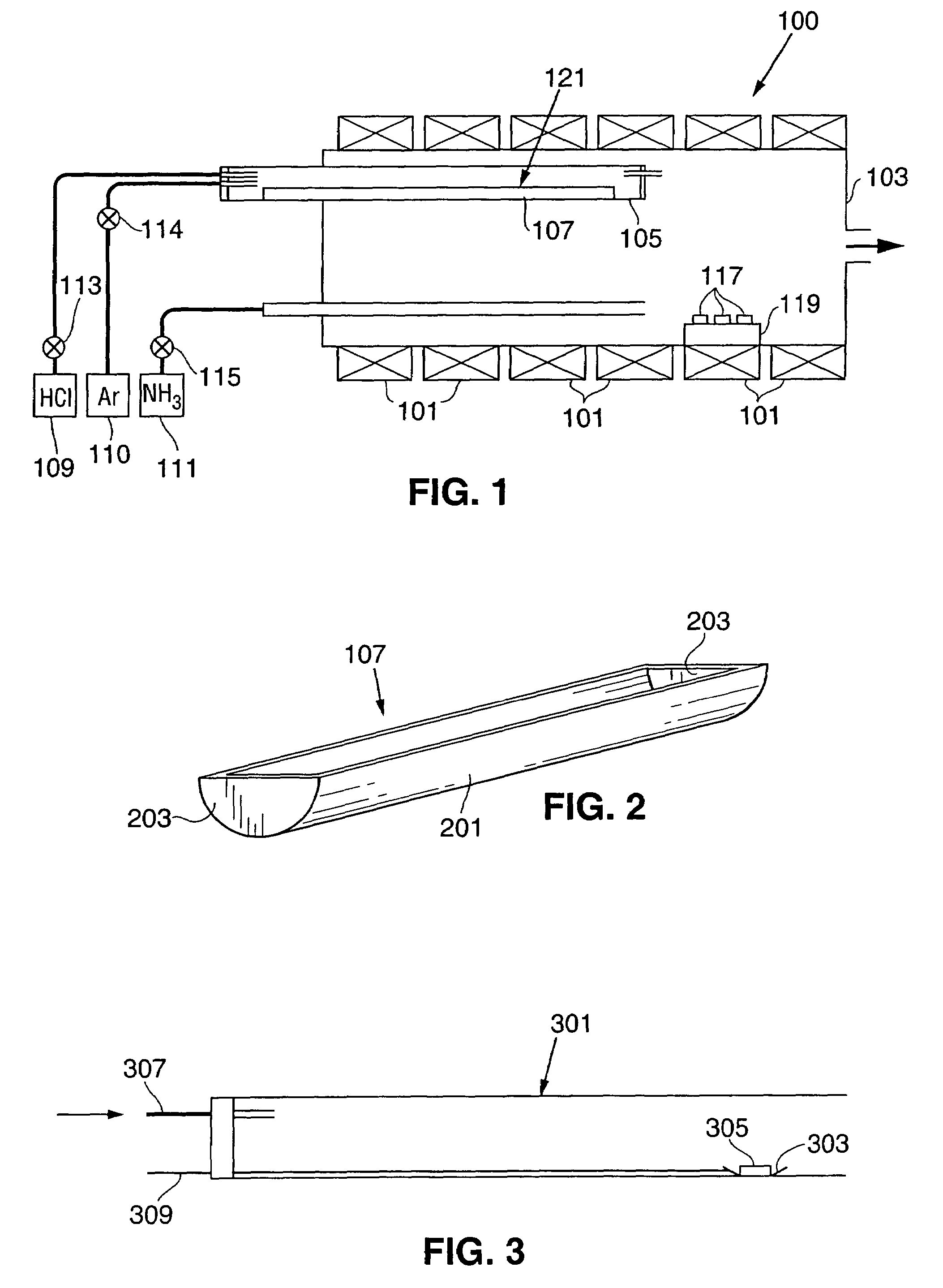
[0054]In this embodiment, multiple SiC substrates of a 6H polytype were loaded into the growth zone of a reactor similar to that shown in FIG. 1. The substrates were placed on a quartz sample holder with the (0001) Si on-axis surface positioned for GaN deposition. One kilogram of Ga metal was positioned in the source boat within the Ga source tube. After purging the reactor with Ar gas to remove air, the growth zone and the Ga source zone were heated to 1100° C. and 650° C., respectively. The majority of the Ga source, however, was maintained at a temperature of less than 100° C., typically in the...
PUM
Property
Measurement
Unit
growth temperature
aaaaa
aaaaa
temperature
aaaaa
aaaaa
temperature
aaaaa
aaaaa
Abstract
An apparatus for growing bulk GaN and AlGaN single crystal boules, preferably using a modified HVPE process, is provided. The single crystal boules typically have a volume in excess of 4 cubic centimeters with a minimum dimension of approximately 1 centimeter. If desired, the bulk material can be doped during growth to achieve n-, i-, or p-type conductivity. In order to have growth cycles of sufficient duration, preferably an extended Ga source is used in which a portion of the Ga source is maintained at a relatively high temperature while most of the Ga source is maintained at a temperature close to, and just above, the melting temperature of Ga. To grow large boules of AlGaN, preferably multiple Al sources are used, the Al sources being sequentially activated to avoid Al source depletion and excessive degradation. In order to achieve high growth rates, preferably a dual growth zone reactor is used in which a first, high temperature zone is used for crystal nucleation and a second, low temperature zone is used for rapid crystal growth. Although the process can be used to grow crystals in which the as-grown material and the seed crystal are of different composition, preferably the two crystalline structures have the same composition, thus yielding improved crystal quality.
Description
PRIORITY CLAIM[0001]The present application is a continuation of U.S. patent application Ser. No. 09 / 903,299, filed Jul. 11, 2001, now U.S. Pat. No. 6,656,285, issued Dec. 2, 2003, which is a continuation of U.S. patent application Ser. No. 09 / 900,833, filed Jul. 6, 2001, now U.S. Pat. No. 6,613,143, issued Sep. 2, 2003.FIELD OF THE INVENTION[0002]The present invention relates generally to semiconductor materials and, more particularly, to an apparatus for growing bulk single crystals.BACKGROUND OF THE INVENTION[0003]Recent results in the development of GaN-based light-emitting diodes (LEDs) and laser diodes (LDs) operating in the green, blue, and ultraviolet spectrum have demonstrated the tremendous scientific and commercial potential of group III nitride semiconductors (e.g., GaN, AlN, InN, and their alloys). These applications require electrically conducting substrates (e.g., GaN or AlGaN) so that a vertical device geometry can be utilized in which the electrodes are located on t...
Claims
Application Information
Patent Timeline
Application Date:The date an application was filed.
Publication Date:The date a patent or application was officially published.
First Publication Date:The earliest publication date of a patent with the same application number.
Issue Date:Publication date of the patent grant document.
PCT Entry Date:The Entry date of PCT National Phase.
Estimated Expiry Date:The statutory expiry date of a patent right according to the Patent Law, and it is the longest term of protection that the patent right can achieve without the termination of the patent right due to other reasons(Term extension factor has been taken into account ).
Invalid Date:Actual expiry date is based on effective date or publication date of legal transaction data of invalid patent.