Semiconductor device and semiconductor memory using the same

a semiconductor and semiconductor technology, applied in solid-state devices, transistors, instruments, etc., can solve the problems of inability to study the softness inability to achieve constant width of the gate channel of the transistor, and ineffective i-type gate for obtaining the body contact in the soi substrate, etc., to achieve the effect of easing the soft error problem, reducing the number of body contact positions, and reducing the number of transistors

Inactive Publication Date: 2007-10-09
SEIKO EPSON CORP
View PDF13 Cites 2 Cited by
  • Summary
  • Abstract
  • Description
  • Claims
  • Application Information

AI Technical Summary

Benefits of technology

[0006]Another advantage of the invention is to provide a semiconductor device and a semiconductor memory using the semiconductor device capable of easing the soft error problems caused by such as α lays, γ lays, or neutrons by modifying the shape of gates.
[0007]Still another advantage of the invention is to provide a semiconductor device and a semiconductor memory using the semiconductor device having a larger freedom of the body contact positions for transistors on the SOI substrates.
[0008]An exemplary semiconductor device according to one aspect of the invention can include, in a field region, a gate, a gate insulating film disposed right under the gate, a body region disposed right under the gate insulating film, and source / drain regions formed on both sides of the body region, wherein the gate comprises a first section extending on the field region along the channel width direction, and a pair of second sections formed on both ends of the first section in the channel width direction and extending along the channel length direction, and is formed as an H-type gate in plan view. According to the semiconductor device of the invention, as long as a part of each of the pair of second sections of the H-type gate is formed on the field region having a constant length in the channel length direction, the channel width can be defined by the length of the first section even if there is a relative position shift between a mask for forming the field region and a mask for forming the gate pattern. As a result, the channel width can be provided as designed.
[0009]In the exemplary semiconductor device according to the invention, the H-type gate can be implemented, thus enabling the gate capacitance to be set larger than those of I-type gates or T-type gates having the same channel width and the same channel length. The larger gate capacitance is generally disadvantageous in view of the operation speed and power consumption. However, it is advantageous for addressing the problems that can be solved by delaying operations of the transistors. For example, it is effective for a measure against soft errors. By delaying operations of transistors, the inversion speed of the signal potential in response to entrance of a single-shot α lay is slowed to provide time for recombination of the charge generated by the α lay prior to the complete inversion of the potential, thus contributing to avoid the signal potential inversion.
[0010]In the semiconductor device according to the invention, the field region can be formed on a SOI substrate. In this case, a body contact can be disposed on the field region across one of the pair of second sections of the H-type gate from the first section. In particular, even if a low resistance layer is formed on a surface of the field region, the body contact region can be separated and insulated from the source / drain region by the second section. Further, since the body contact region can be disposed adjacent either one of the pair of second sections of the H-type gate, larger freedom of the layout of the body contact region than the conventional T-type gates can be provided.
[0011]In the semiconductor device according to the invention, the field region can be formed on a bulk substrate. In case of the bulk substrate, except for the point that the body contact regions are not necessary for every transistor, the H-type gate functions as measures for the mask shift and the soft error as is the case with the SOI substrate.

Problems solved by technology

However, I-type gates are not effective for obtaining the body contact in SOI substrates.
However, there is a disadvantage that the width of the gate channels of transistors cannot be made constant if the mask shift occurs.
Further, it has not been studied to ease the soft error problems caused by such as α lays, γ lays, or neutrons by modifying the shape of gates.

Method used


Image

  • Semiconductor device and semiconductor memory using the same
  • Semiconductor device and semiconductor memory using the same
  • Semiconductor device and semiconductor memory using the same

Examples


Embodiment Construction

[0024]Hereinafter, an exemplary embodiment of the invention is described referring to the accompanying drawings.

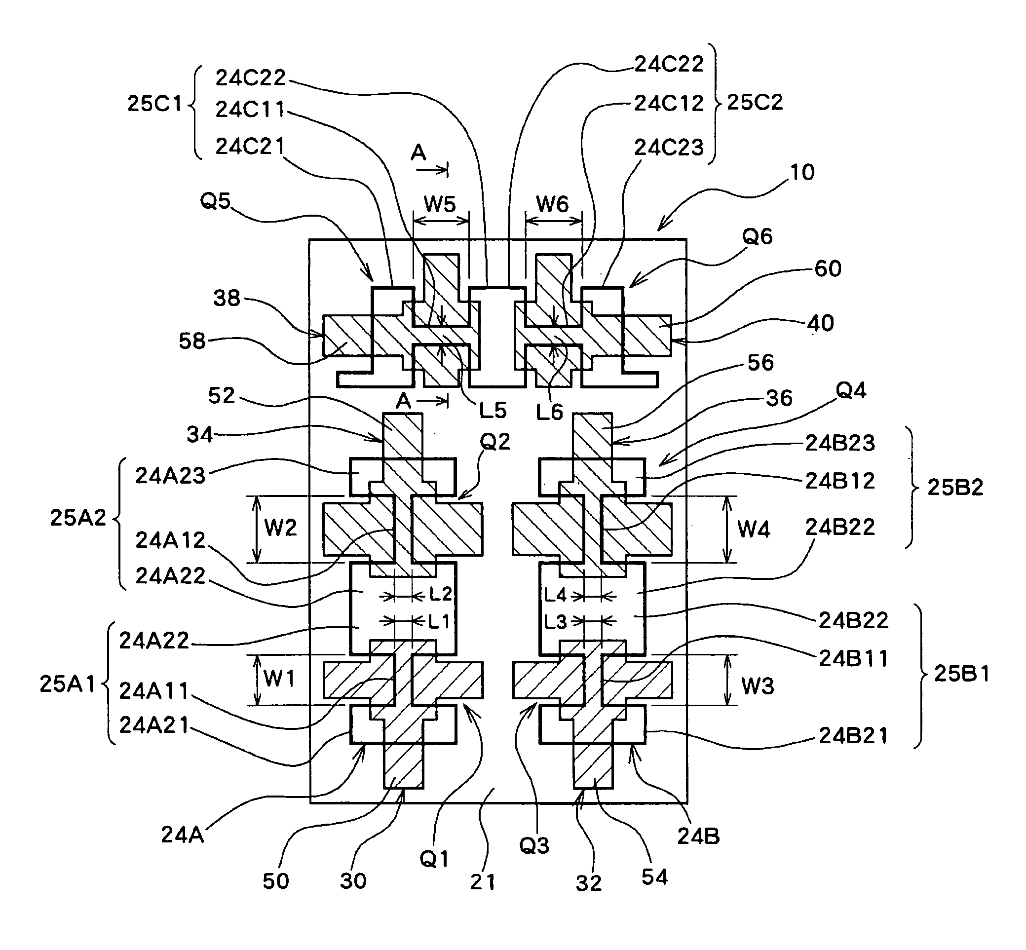
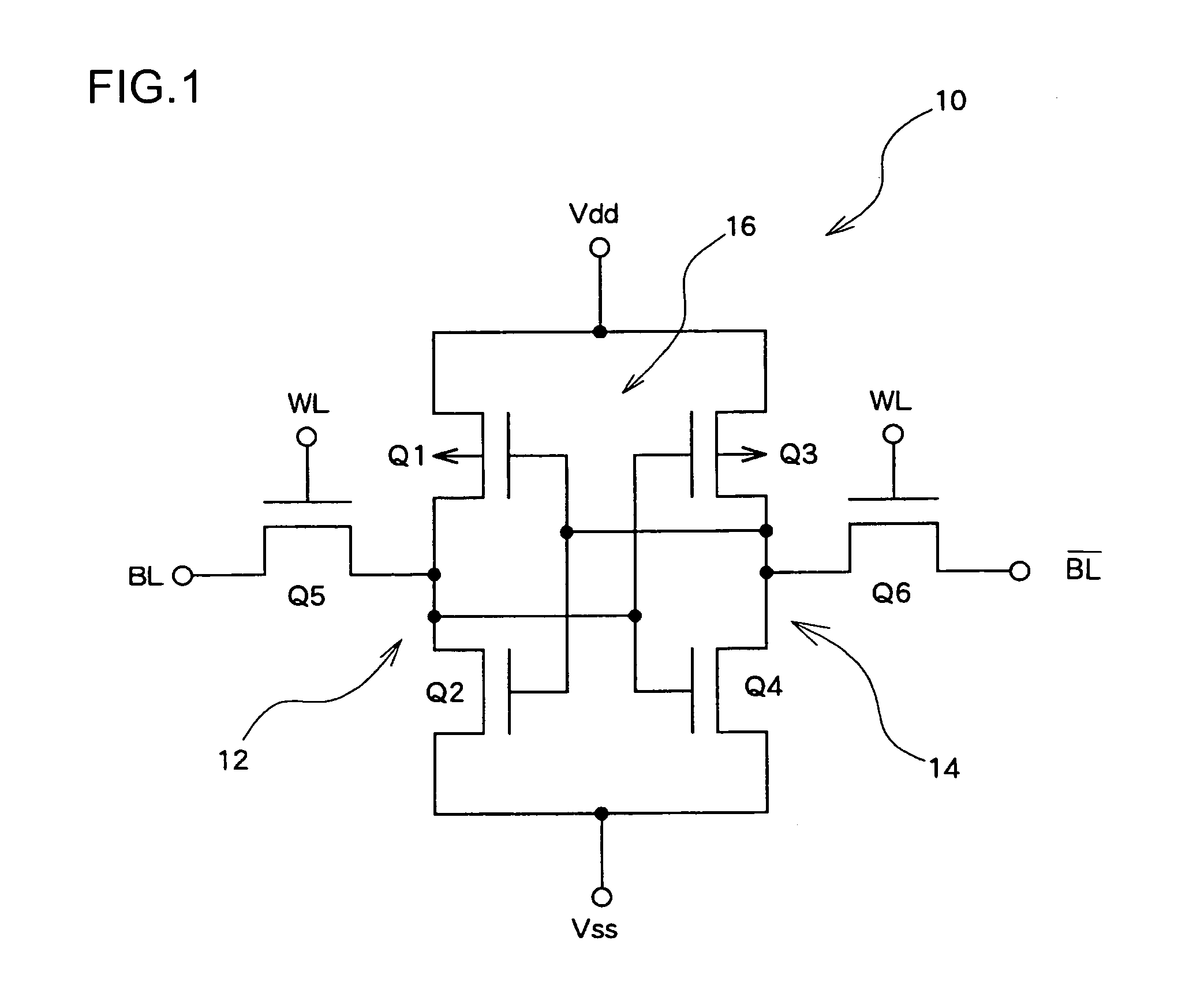
[0025]FIG. 1 is an equivalent circuit of one of memory cells of an SRAM as an exemplary semiconductor memory according to the invention. A memory cell 10 of the SRAM is composed of six MOS field effect transistors. One P-channel load transistor Q1 and one N-channel drive transistor Q2 serially connected thereto form a first CMOS inverter 12. The other P-channel load transistor Q3 and the other N-channel drive transistor Q4 connected in series thereto form a second CMOS inverter 14. A Vdd power source line is connected to the sources of the pair of P-channel load transistors Q1, Q3 while a Vss power source line is connected to the sources of the pair of N-channel drive transistors Q2, Q4. And, by cross-coupling the first and the second CMOS inverters, a flip-flop 16 is formed. The flip-flop 16 is connected to a bit line BL and an inverted bit line BL via pair of N-channel t...


PUM


Abstract

Aspects of the invention can provide a semiconductor device and a semiconductor memory using the semiconductor device having a gate shape by which the width of the gate can be realized as designed even if relative shifts occur between the masks for forming the field regions and the gate patterns. The semiconductor device can include, in field regions, a gate (an H-type gate), a gate insulating film right under the gate, a body region right under the gate insulating film, and source / drain regions formed on both sides of and across the body region. The H-type gate can have a first section extending along the channel width direction on the field region, and a pair of second sections formed on both ends of the first section in the channel width direction and extending along the channel length direction, and is formed to be an H shape in plan view. Since a part of each of the pair of second sections of the H-type gate can be formed on a part of the field region having a constant length in the channel length direction, the channel width can be defined by the length of the first section.

Description

BACKGROUND OF THE INVENTION[0001]1. Field of Invention[0002]Aspects of the invention relate to a semiconductor device formed on a SOI (Silicon On Insulator) substrate or on a bulk substrate and a semiconductor memory using the semiconductor device.[0003]2. Description of Related Art[0004]As a shape of the gate on related field of transistors, in addition to the I-type gate used for bulk substrates, the T-type gate used for obtaining the body contact in the SOI substrates can be used. I-type gates are advantageous in that they have small gate capacitance and that they require the minimum sell areas. However, I-type gates are not effective for obtaining the body contact in SOI substrates. In this respect, the T-type gates are effective for separating the source / drain regions from the body contact regions even if the surfaces of field regions in SOI substrates are formed of silicide layers. However, there is a disadvantage that the width of the gate channels of transistors cannot be ma...

Claims


Application Information

Patent Timeline
Patent Type & Authority Patents(United States)
IPC IPC(8): H01L27/01H01L27/12H01L31/0392H01L27/10G11C11/412H01L21/8244H01L27/02H01L27/11H01L29/786
CPCG11C11/412H01L27/1203H01L27/1104H01L27/0207H10B10/12
Inventor TAGUCHI, KAZUO
Owner SEIKO EPSON CORP
Why Eureka
Try Eureka