
Method for differential-mode processing of an incident voltage relative to a reference voltage and corresponding device

a voltage signal and incident voltage technology, applied in the direction of dc-amplifiers with dc-coupled stages, dc-amplifiers controlled by light, amplifiers, etc., can solve the problems of incompatibility with the input range of voltage/current converters, high current level, and relatively complex approach, etc., to achieve easy operation, facilitate operation, and improve stability

Inactive Publication Date: 2007-10-09
STMICROELECTRONICS SRL
View PDF5 Cites 7 Cited by
  • Summary
  • Abstract
  • Description
  • Claims
  • Application Information

AI Technical Summary

Benefits of technology

This approach effectively transforms incident voltage into a compatible range for analog-digital converters, enhancing noise rejection and stability, while simplifying the circuit structure and reducing harmonic distortion.

Problems solved by technology

This quantity of light can vary because of defects in optical disks and voltage offsets generated by the various components of the circuit.
But, at the output of the current / current converter, the current level can be very high and incompatible with the input range of the voltage / current converter.
However, such an approach turns out to be relatively complex to implement.
Moreover, such a processing circuit is a source of harmonic distortion.
In addition, it has a relatively low noise-rejection ratio and the structure has a stability problem at very high frequency.

Method used


Image

  • Method for differential-mode processing of an incident voltage relative to a reference voltage and corresponding device
  • Method for differential-mode processing of an incident voltage relative to a reference voltage and corresponding device
  • Method for differential-mode processing of an incident voltage relative to a reference voltage and corresponding device

Examples


Embodiment Construction

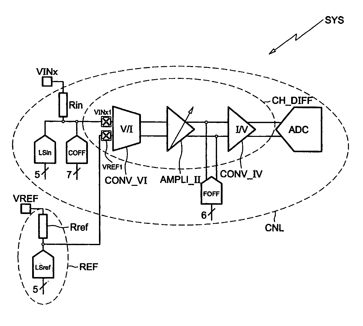
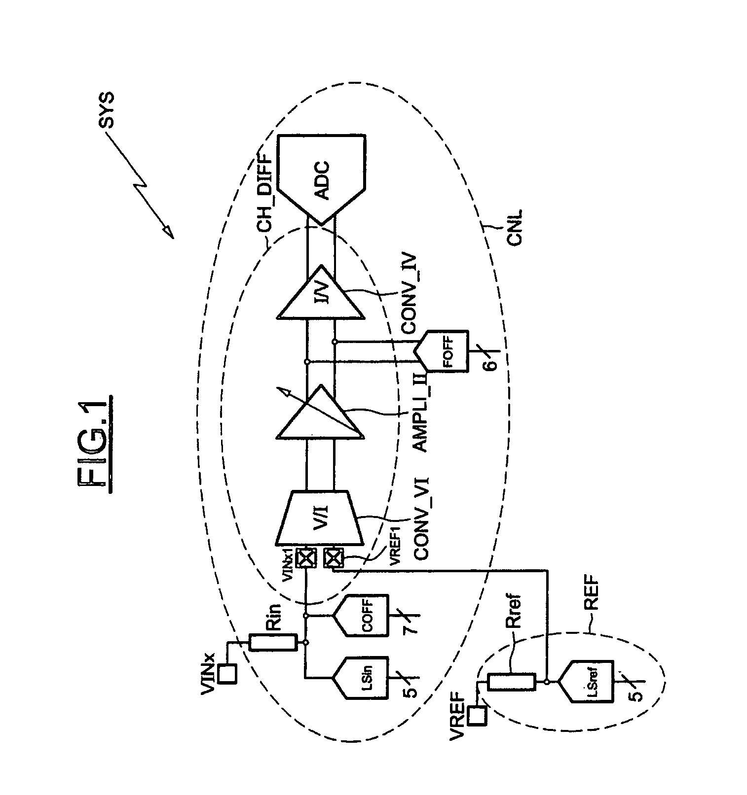
[0024]A system SYS according to the invention is shown in FIG. 1. In the example described here, this device is connected to the output of a photodetector (not shown) that is integrated, for example, into an optical disk reader system, such as an audio or video digital disk. The photodetector comprises an optical lens divided into several quadrants. The number of quadrants depends on the type of optical lens used. Each quadrant of the optical lens generates an incident voltage signal VINx, representing the data item read by the reader system.

[0025]The reference CNL represents a channel of the device according to the invention designed to process the signal VINx generated by one quadrant of the optical lens. There are therefore as many channels CNL as there are signals generated by the optical lens. To simplify the figure, only one channel CNL is shown. The block REF allows a reference signal VREF, characteristic of the reader system, to be generated. The signal VREF is identical for...


PUM


Abstract

A device for differential-mode processing of an incident voltage relative to a reference voltage includes a differential circuit including a voltage / current conversion block having a differential input, designed to receive the incident voltage at a first input and the reference voltage at a second input. A current amplification block includes a gain module and a current subtraction module. A current / voltage conversion block includes an operational amplifier with differential transimpedance supplied with a common-mode voltage, receiving the two currents output from the amplification block at its input, and delivering two calibrated opposing voltages at its output that are centered around the common-mode voltage.

Description

FIELD OF THE INVENTION[0001]The invention relates to voltage signal processing circuits, in particular those designed to deliver, from an incident signal, an output signal in a predetermined voltage range.BACKGROUND OF THE INVENTION[0002]The invention may be applied advantageously, but is not limited to, the reading of an optical signal, in particular in optical disk reader systems. In these systems, the processing circuit is situated between a photodetector and an analog-digital converter to adapt the signal coming from the photodetector to the input range of the analog-digital converter. The amplitude of the incident voltage can vary depending on the quantity of light emitted by the reader system laser and received by the processing circuit. This quantity of light can vary because of defects in optical disks and voltage offsets generated by the various components of the circuit.[0003]An approach developed by the Applicant in the Patent FR-2 820 307 proposes an asymmetric processin...

Claims


Application Information

Patent Timeline
Patent Type & Authority Patents(United States)
IPC IPC(8): H03F3/08
CPCH03F3/45183H03F3/68H03F3/45659
Inventor GRILLO, LIONELTHIES, WILLIAM
Owner STMICROELECTRONICS SRL
Learn More