Eureka AIR delivers breakthrough ideas for toughest innovation challenges, trusted by R&D personnel around the world.

Ion doping method to form source and drain

Inactive Publication Date: 2007-10-16
GRACE SEMICON MFG CORP
View PDF1 Cites 0 Cited by
  • Summary
  • Abstract
  • Description
  • Claims
  • Application Information

AI Technical Summary

Benefits of technology

[0007]An objective of the present invention is to provide an ion doping method to form source and drain, which uses a Y-shaped polysilicon layer, gate spacer and dielectric layer to be as a barrier layer when ions implanted, so as to make ions implanted into a semiconductor substrate diffuse naturally to form heavily doped source / drain regions and lightly doped source / drain regions in order to obtain a better ion doping profile of source and drain and to keep a better channel length.
[0008]Another objective of the present invention is to provide an ion doping method to form source and drain, which effectively controls a channel length and the size of the overlapping regions between doped regions and a gate structure, so as to be suitable for components minimized at the deep submicron manufacturing process.

Problems solved by technology

These will make the manufacturing process, such as the photomask pattern transfer, ion implantation and deposition, more difficult.
At this time, electrons easily penetrate the extension regions to lead to leakage current.

Method used


Image

  • Ion doping method to form source and drain
  • Ion doping method to form source and drain
  • Ion doping method to form source and drain

Examples


Embodiment Construction

[0013]The present invention relates an ion doping method to form source and drain. This method is suitable to the component manufacturing at the deep submicron scale, and thus makes a gate obtain a nice ion doping profile of source / drain regions and a good channel length at such a small scale.

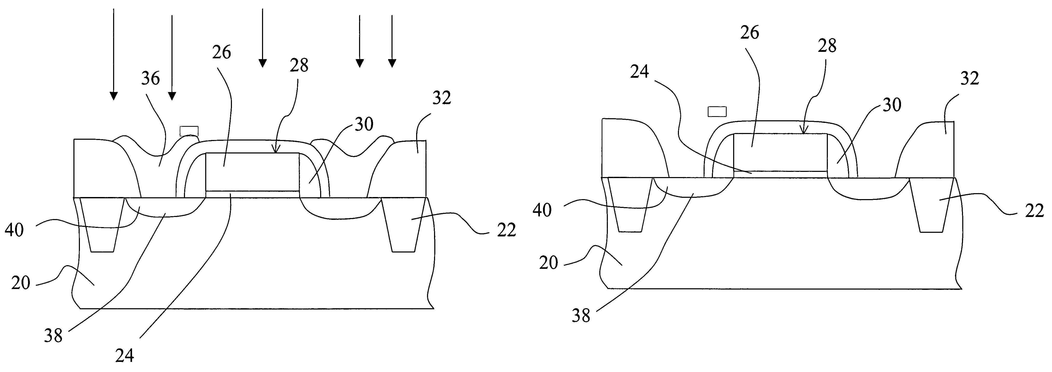
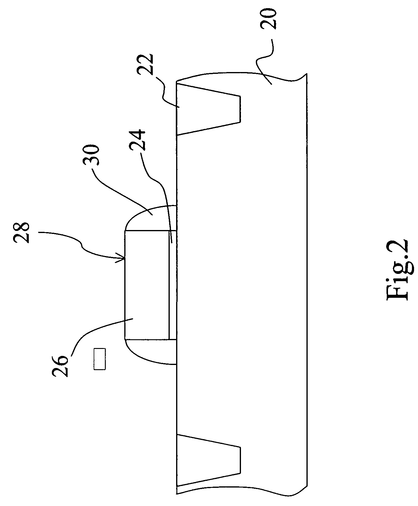
[0014]First, referring to FIG. 2, a plurality of shallow trench isolations (STI) 22 are formed in the semiconductor substrate 20 to isolate active devices and passive ones in the semiconductor substrate 20. Then, a gate oxide layer 24 is formed on the surface of the semiconductor substrate 20, and a polysilicon layer 26 is formed on gate oxide layer 24. Thus, a transistor gate structure 28, which includes gate oxide layer 24 and polysilicon layer 26, is formed. Later, a silicon nitride layer is formed on the semiconductor substrate 20 by chemical vapor deposition, and then a dry etching process of reactive ion etching is performed on the silicon nitride layer to form a gate spacer 30.

[0015]A di...


PUM


Abstract

An ion doping method to form source and drain is disclosed. First form a gate structure and a gate spacer on a semiconductor substrate, and then use dielectric layer having trenches therein to define heavily ion-doped positions and use a Y-shaped polysilicon layer formed in the trenches. Perform an ion implantation, by using the polysilicon layer, gate spacer and dielectric layer as a barrier layer, to naturally form ion doped regions of source / drain, so as to make components, which are minimized in the increased packing density, still have a gate structure keeping an enough channel length.

Description

BACKGROUND OF THE INVENTION[0001]1. Field of the Invention[0002]The present invention relates to an ion doping method to form source and drain, and more particularly to an ion doping method suitable to form source and drain at the deep submicron scale.[0003]2. Description of the Related Art[0004]With the progress of the semiconductor technology, the number of components on per unit area of a wafer increases according to Moore's law. Yet the density distribution of transistors becomes higher and higher, and the size of components becomes smaller and smaller. These will make the manufacturing process, such as the photomask pattern transfer, ion implantation and deposition, more difficult.[0005]After the junction of a gate and source / drain becomes shallow at the deep submicron scale, the doping profile of shallow or deep ions is the main key to control the short channel effect and device driving characteristics. The conventional manufacturing process is shown in FIG. 1. First, ions are...

Claims


Application Information

Patent Timeline
IPC IPC(8): H01L21/336
CPCH01L21/2652H01L29/66598H01L21/266Y10S438/976
Inventor TSAI, NAN-HSIUNG
Owner GRACE SEMICON MFG CORP
Why Eureka
Eureka Blog
Learn More